
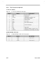


3-12
Service Guide
The valid values for this timer range from 1 to 15 minutes with default set at
[1]
. Select
[Off]
to disable the timer.
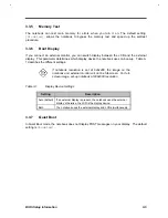
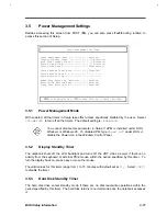
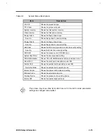
3.5.4
System Sleep Timer
This parameter enables you to set a timeout period for the notebook to enter either standby or
hibernation mode. The System Sleep Mode parameter determines which sleep mode the
notebook will enter into.
The valid values for this timer range from 1 to 15 minutes with default set at
[3]
. Select
[Off]
to disable the timer.
3.5.5
System Sleep Mode
This parameter tells the notebook which sleep mode (Standby or Hibernation) to enter into when
the System Sleep Timer times out. The default setting is
[Hibernation]
.
3.5.6
System Resume Timer Mode
When enabled, the notebook resumes from standby mode at the specified Resume Date and
Resume Time parameter settings.
When the notebook is in hibernation mode, it cannot resume when this
parameter is enabled.
3.5.7
System Resume Date and Time
The Resume Date and Resume Time parameters let you set the date and time for the resume
operation. The date and time fields take the same format as the System Date and Time
parameters in the Basic System Settings screen.
Setting a resume date and time that is not valid automatically disables these
fields. A successful resume occurring from a date and time match
automatically disables these fields.
3.5.8
Modem Ring Resume On Indicator
When enabled, the notebook wakes up from standby mode and returns to normal mode when a
PCMCIA modem detects a ringing tone. The default setting is
[Enabled]
.
When the notebook is in hibernation mode, it cannot resume from a modem
ring.
Содержание AcerNote Light 370P
Страница 1: ...TI Extensa 61X Series AcerNote 370P Notebook Service Guide PART NO 2238309 0809 DOC NO PRINTED IN USA ...
Страница 6: ...vi ...
Страница 26: ...1 8 Service Guide Figure 1 5 Main Board Layout Bottom Side ...
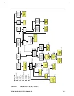
Страница 49: ...System Introduction 1 31 1 5 1 3 Power Management Figure 1 14 Power Management Block Diagram ...
Страница 55: ...System Introduction 1 37 1 6 System Block Diagram Figure 1 15 System Block Diagram ...
Страница 64: ...Major Chips Description 2 7 2 2 5 Pin Diagram Figure 2 4 M1521 Pin Diagram ...
Страница 99: ...2 42 Service Guide 2 5 3 Pin Diagram Figure 2 10 C T 65550 Pin Diagram ...
Страница 116: ...Major Chips Description 2 59 2 6 4 Block Diagram Figure 2 11 Functional Block Diagram 16 bit PC Card Interface ...
Страница 117: ...2 60 Service Guide Figure 2 12 Functional block diagram CardBus Card Interface ...
Страница 118: ...Major Chips Description 2 61 2 6 5 Pin Diagram Figure 2 13 PCI to PC Card 16 bit terminal assignments ...
Страница 119: ...2 62 Service Guide Figure 2 14 PCI to CardBus terminal assignments ...
Страница 135: ...2 78 Service Guide 2 7 3 Pin Diagram Figure 2 16 NS87336VJG Pin Diagram ...
Страница 145: ...2 88 Service Guide 2 8 2 Pin Diagram Figure 2 17 YMF715 Block Diagram ...
Страница 185: ...Disassembly and Unit Replacement 4 5 Figure 4 3 Disassembly Sequence Flowchart ...
Страница 209: ...B 2 Service Guide ...
Страница 210: ...Exploded View Diagram B 3 ...
Страница 217: ...A p p e n d i x D A p p e n d i x D Schematics This appendix shows the schematic diagrams of the notebook ...


