3-6
Service Guide
3.4
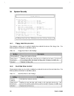
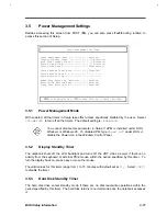
System Security
System Security
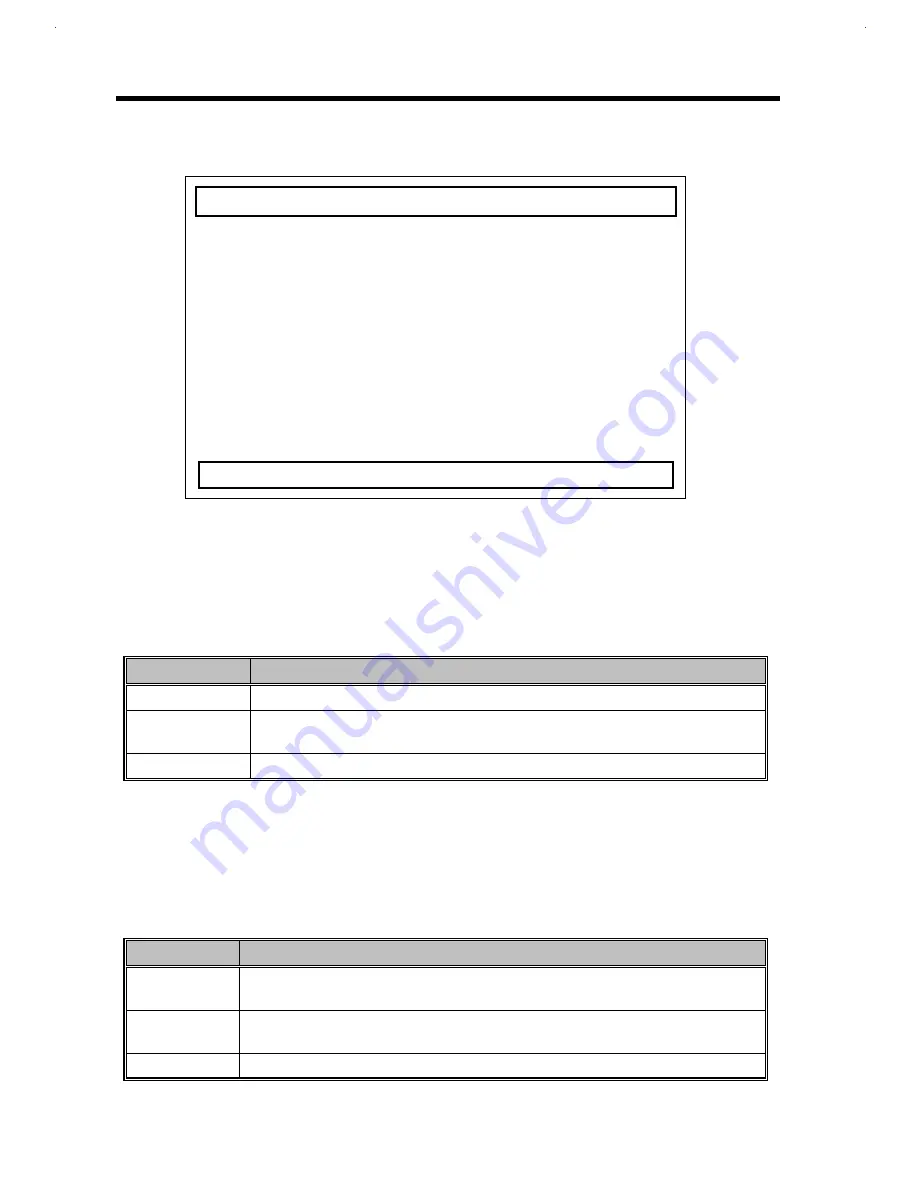
Disk Drive Control
Floppy Disk Drive ------------- [Normal]
Hard Disk Drive --------------- [Normal]
System Boot Drive ------------- [Drive A Then C]
CD-ROM Bootable --------------- [Disabled]
On Board Communication Ports
Serial Port 1 Base Address ---- [3F8h(IRQ 4)]
Parallel Port Base Address ---- [378h(IRQ 7)]
Parallel Port Operation Mode -- [Standard and Bidirectional]
ECP DMA Channel -------------- [0]
Setup Password ------------------- [None]
Power On Password ---------------- [None]
Plug and Play O/S ---------------- [Yes]
OS Legacy Mode Support ----------- [Disabled]
↑↓
=Move Highlight Bar,
→←
=Change Setting, F1=Help, Esc=Exit
3.4.1
Floppy Disk Drive Control
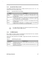
This parameter allows you to enable or disable the read/write functions of the floppy drive. The
following table summarizes the available options.
Table 3-2
Floppy Disk Drive Control Settings
Setting
Description
Normal (default)
Floppy drive functions normally
Write Protect
Boot Sector
Disables the floppy drive write function on a diskette’s boot sector. This option is
for operating systems that access the floppy drive 100 percent via BIOS only.
Disabled
Disables the floppy drive
3.4.2
Hard Disk Drive Control
This parameter allows you to enable or disable the read/write functions of the hard disk drive. The
following table summarizes the available options.
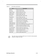
Table 3-3
Hard Disk Drive Control Settings
Setting
Description
Normal
(default)
Hard disk drive functions normally
Write Protect
Boot Sector
Disables the hard disk drive write function on the hard disk’s boot sector. This
option is for operating systems that access the hard disk 100 percent via BIOS only.
Disabled
Disables the hard disk drive
Содержание AcerNote Light 370P
Страница 1: ...TI Extensa 61X Series AcerNote 370P Notebook Service Guide PART NO 2238309 0809 DOC NO PRINTED IN USA ...
Страница 6: ...vi ...
Страница 26: ...1 8 Service Guide Figure 1 5 Main Board Layout Bottom Side ...
Страница 49: ...System Introduction 1 31 1 5 1 3 Power Management Figure 1 14 Power Management Block Diagram ...
Страница 55: ...System Introduction 1 37 1 6 System Block Diagram Figure 1 15 System Block Diagram ...
Страница 64: ...Major Chips Description 2 7 2 2 5 Pin Diagram Figure 2 4 M1521 Pin Diagram ...
Страница 99: ...2 42 Service Guide 2 5 3 Pin Diagram Figure 2 10 C T 65550 Pin Diagram ...
Страница 116: ...Major Chips Description 2 59 2 6 4 Block Diagram Figure 2 11 Functional Block Diagram 16 bit PC Card Interface ...
Страница 117: ...2 60 Service Guide Figure 2 12 Functional block diagram CardBus Card Interface ...
Страница 118: ...Major Chips Description 2 61 2 6 5 Pin Diagram Figure 2 13 PCI to PC Card 16 bit terminal assignments ...
Страница 119: ...2 62 Service Guide Figure 2 14 PCI to CardBus terminal assignments ...
Страница 135: ...2 78 Service Guide 2 7 3 Pin Diagram Figure 2 16 NS87336VJG Pin Diagram ...
Страница 145: ...2 88 Service Guide 2 8 2 Pin Diagram Figure 2 17 YMF715 Block Diagram ...
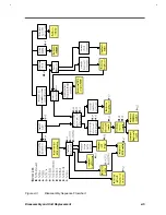
Страница 185: ...Disassembly and Unit Replacement 4 5 Figure 4 3 Disassembly Sequence Flowchart ...
Страница 209: ...B 2 Service Guide ...
Страница 210: ...Exploded View Diagram B 3 ...
Страница 217: ...A p p e n d i x D A p p e n d i x D Schematics This appendix shows the schematic diagrams of the notebook ...


