


BIOS Setup Information
3-5
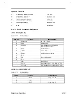
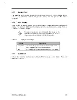
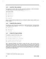
3.3.5
Memory Test
The notebook can test main memory for errors when you turn it on. The default setting,
[Disabled]
, allows the notebook to bypass the memory test and speed up the self-test
procedure.
3.3.6
Boot Display
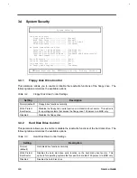
If you connect an external monitor, you can switch display between the LCD and the external
display. This parameter determines which display device the notebook uses on boot-up. Table 3-
1 describes the different settings.
If notebook resolution is set at 640x480, the image on the
notebook and external monitor will not be full-screen. For full-
screen image, set-up notebook at 800x600 resolution.
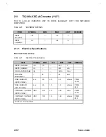
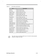
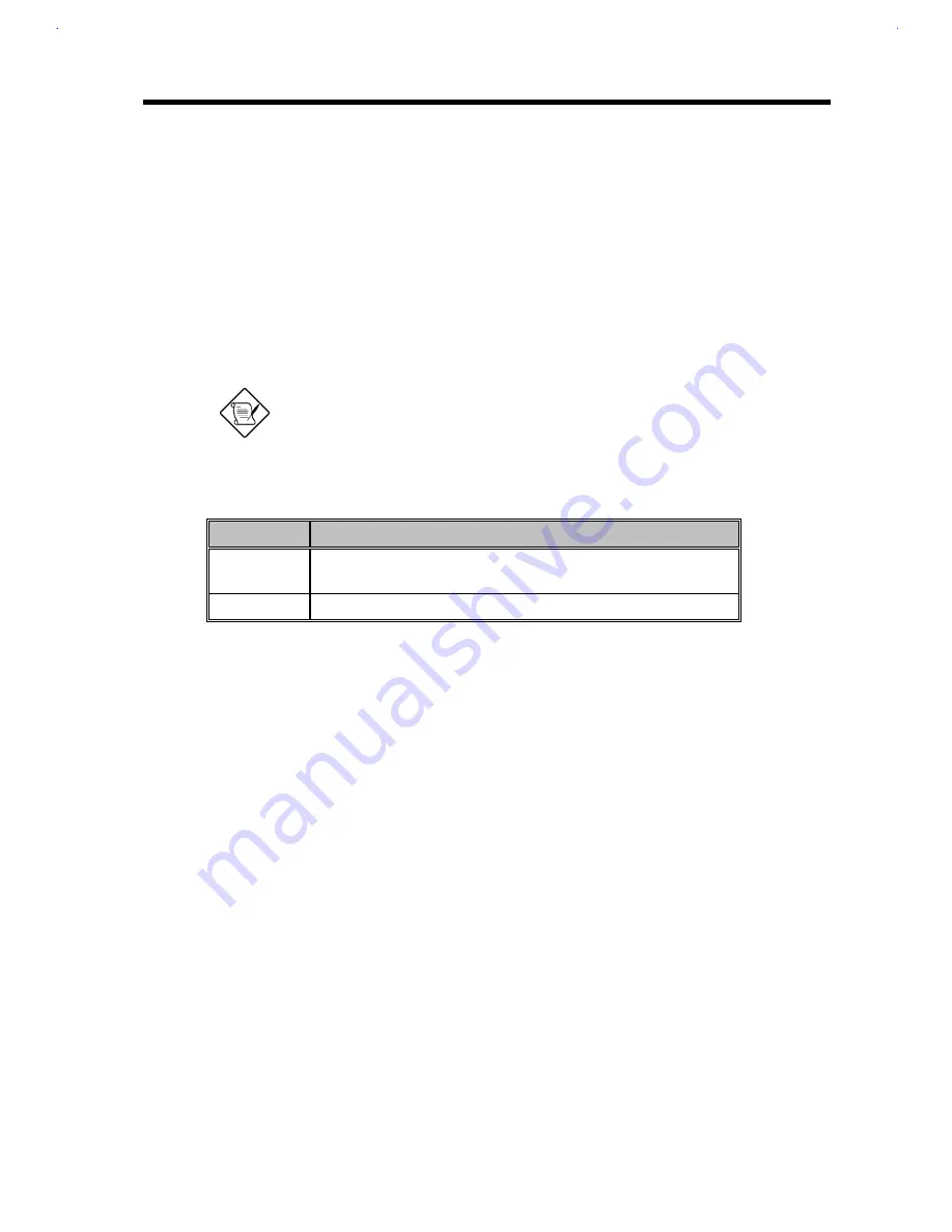
Table 3-1
Display Device Settings
Setting
Description
Auto (default)
If an external display is present, the notebook uses the external
display; otherwise, the LCD is the display device.
Both
The notebook uses the external display and LCD simultaneously.
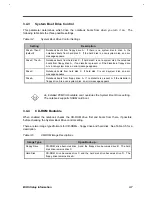
3.3.7
Quiet Boot
In Quiet Boot mode, the notebook does not display POST messages on your display. The default
setting is
[Enabled]
.
Содержание AcerNote Light 370P
Страница 1: ...TI Extensa 61X Series AcerNote 370P Notebook Service Guide PART NO 2238309 0809 DOC NO PRINTED IN USA ...
Страница 6: ...vi ...
Страница 26: ...1 8 Service Guide Figure 1 5 Main Board Layout Bottom Side ...
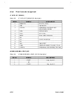
Страница 49: ...System Introduction 1 31 1 5 1 3 Power Management Figure 1 14 Power Management Block Diagram ...
Страница 55: ...System Introduction 1 37 1 6 System Block Diagram Figure 1 15 System Block Diagram ...
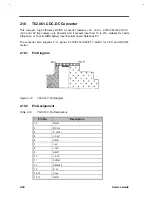
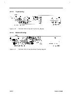
Страница 64: ...Major Chips Description 2 7 2 2 5 Pin Diagram Figure 2 4 M1521 Pin Diagram ...
Страница 99: ...2 42 Service Guide 2 5 3 Pin Diagram Figure 2 10 C T 65550 Pin Diagram ...
Страница 116: ...Major Chips Description 2 59 2 6 4 Block Diagram Figure 2 11 Functional Block Diagram 16 bit PC Card Interface ...
Страница 117: ...2 60 Service Guide Figure 2 12 Functional block diagram CardBus Card Interface ...
Страница 118: ...Major Chips Description 2 61 2 6 5 Pin Diagram Figure 2 13 PCI to PC Card 16 bit terminal assignments ...
Страница 119: ...2 62 Service Guide Figure 2 14 PCI to CardBus terminal assignments ...
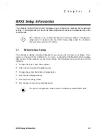
Страница 135: ...2 78 Service Guide 2 7 3 Pin Diagram Figure 2 16 NS87336VJG Pin Diagram ...
Страница 145: ...2 88 Service Guide 2 8 2 Pin Diagram Figure 2 17 YMF715 Block Diagram ...
Страница 185: ...Disassembly and Unit Replacement 4 5 Figure 4 3 Disassembly Sequence Flowchart ...
Страница 209: ...B 2 Service Guide ...
Страница 210: ...Exploded View Diagram B 3 ...
Страница 217: ...A p p e n d i x D A p p e n d i x D Schematics This appendix shows the schematic diagrams of the notebook ...


