


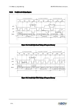


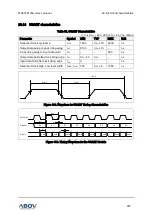

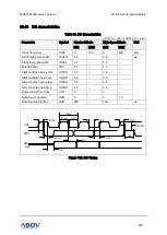


20. Electrical characteristics
MC97F6108A User’s manual
222
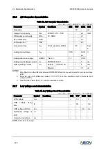
20.6
A/D Converter characteristics
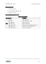
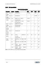
Table 43. A/D Converter Characteristics
(T
A
=-40°C ~ +85°C, VDD=2.7V ~ 5.5V, VSS=0V)
Parameter
Symbol
Conditions
MIN
TYP
MAX Unit
Resolution
–
–
–
12
–
bit
Integral non-linearity
INL
AVREF=2.7V ~ 5.5V
fx = 8MHz
–
–
±4
LSB
Differential non-linearity
DNL
–
–
±1
Zero offset error
ZOE
–
–
±7
Full scale error
FSE
–
–
±3
Conversion time
t
CON
12-bit resolution, 8MHz
–
60
–
Cycl
e
Analog input voltage
V
AN
–
VSS
–
AVR
EF
V
Analog reference voltage
AVREF
*Note 3
2.7
–
VDD
Analog input leakage current I
AN
VDDREF=5.12V
–
–
2
uA
ADC operating current
I
ADC
Enable
VDD=5.12V
–
1
2
mA
Disable
–
–
0.1
uA
NOTES
:
1.
Zero offset error is the difference between 000000000000 and the converted output for zero input voltage
(VSS).
2.
Full scale error is the difference between 111111111111 and the converted output for full-scale input
voltage (AVREF).
3.
When AVREF is lower than 2.7V, the ADC resolution
is worse.
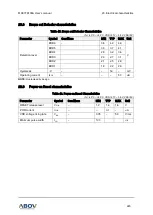
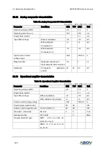
20.7
Low voltage reset characteristics
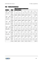
Table 44. Low Voltage Reset Characteristics
(T
A
=-40°C ~ +85°C, VDD=2.7V ~ 5.5V, VSS=0V)
Parameter
Symbol
Conditions
MIN TYP MAX Unit
LVR voltage
V
LVR
–
–
1.8
–
V
VDD voltage rising
time
t
R
–
–
50
–
mV
VDD voltage off time
t
OFF
–
–
–
50
uA
Hysteresis voltage of
LVR
△V
–
–
–
–
–
Current consumption
I
LVR
–
–
–
–
–
NOTE:
Guaranteed by design.