Appendix
A96G140/A96G148/A96A148 User’s manual
268
20.7
Circuit design guide
To program Flash memory, programming tools require 4 signal lines, DSCL, DSDA, VDD, and VSS.
When designing a PCB circuit, you should consider these 4 signal lines for on-board programming. In
addition, you need to be careful when designing the related circuit of these signal pins, because
rising/falling timing of the DSCL and DSDA is very important for proper programming.
When you use the OCD pins exclusively or share them with other functions, it needs to be careful, too.
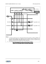
Figure 147 shows an example circuit where the OCD pins (DSCL and DSDA) are shared with other
functions. They must be connected when debugging or executing In System Program (ISP).
Normally, the OCD pins are connected to outside to execute the predefined functions. Even when they
are connected for debugging or executing ISP directly, the OCD pins are shared with other functions
by using resistors as shown in Figure 147. By doing this, the OCD pins process the normal external
signals and execute the OCD functions first when they are shared.


