


Publication No. PPC11A-HRM/1
Functional Description 57
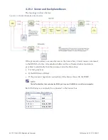
4.20.3 I
2
C Bus 3
The topology is shown below:
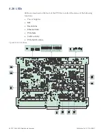
Figure 4-8 I
2
C Bus 3 Structure
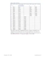
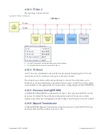
Table 4-28 I
2
C Bus 3 Addresses
Device
7-Bit Address
PCIe Switch 1
0x38 + [0:2]
a
PCIe Switch 2
0x38 + [0:2]
a
PCIe clock synthesizer 1
0x6A
b
PCIe clock synthesizer 2
0x68
b
a.
See the PCIe Switches section and device data sheet for details.
b.
The clock synthesizers are only accessible to Abaco.
4.20.4 I
2
C Reset
An I
2
C bus may potentially lock-up if the reset is applied (stopping the I
2
C clock)
when a slave device (without a reset pin) is driving out data.
The processor provides a software mechanism to recover from this state, so no
hardware recovery mechanism is provided. The processor and PCIe switches apply
a reset pattern to the appropriate I
2
C buses before configuring from their EEPROMs.
4.20.5 Processor Config EEPROM
A 32 KB 24LC256 EEPROM is attached to I
2
C Bus 1. This can store the RCW for the
processor if selected by the software configuration option. The device is write-
enabled only when the
Configuration Write Enable Link
(P15 pins 9 and 10) is fitted.
4.20.6 Elapsed Time Indicator
A Maxim DS1682 Elapsed-Time Indicator logs the amount of time the PPC11A has
been powered and the number of power cycles.
Содержание PPC11A
Страница 1: ...Hardware Reference Manual PPC11A 6U VME Single Board Computer Edition 1 Publication No PPC11A HRM 1 ...
Страница 27: ...Publication No PPC11A HRM 1 Functional Description 27 Figure 4 2 Block Diagram T2081 ...
Страница 113: ...Publication No PPC11A HRM 1 Connectors 113 Figure 6 2 Rear Connector Position ...


