background image

AD484 user manual   


       V1.2 


AD484 User manual 

February 2007                   


www.4dsp.com


- 12 - 


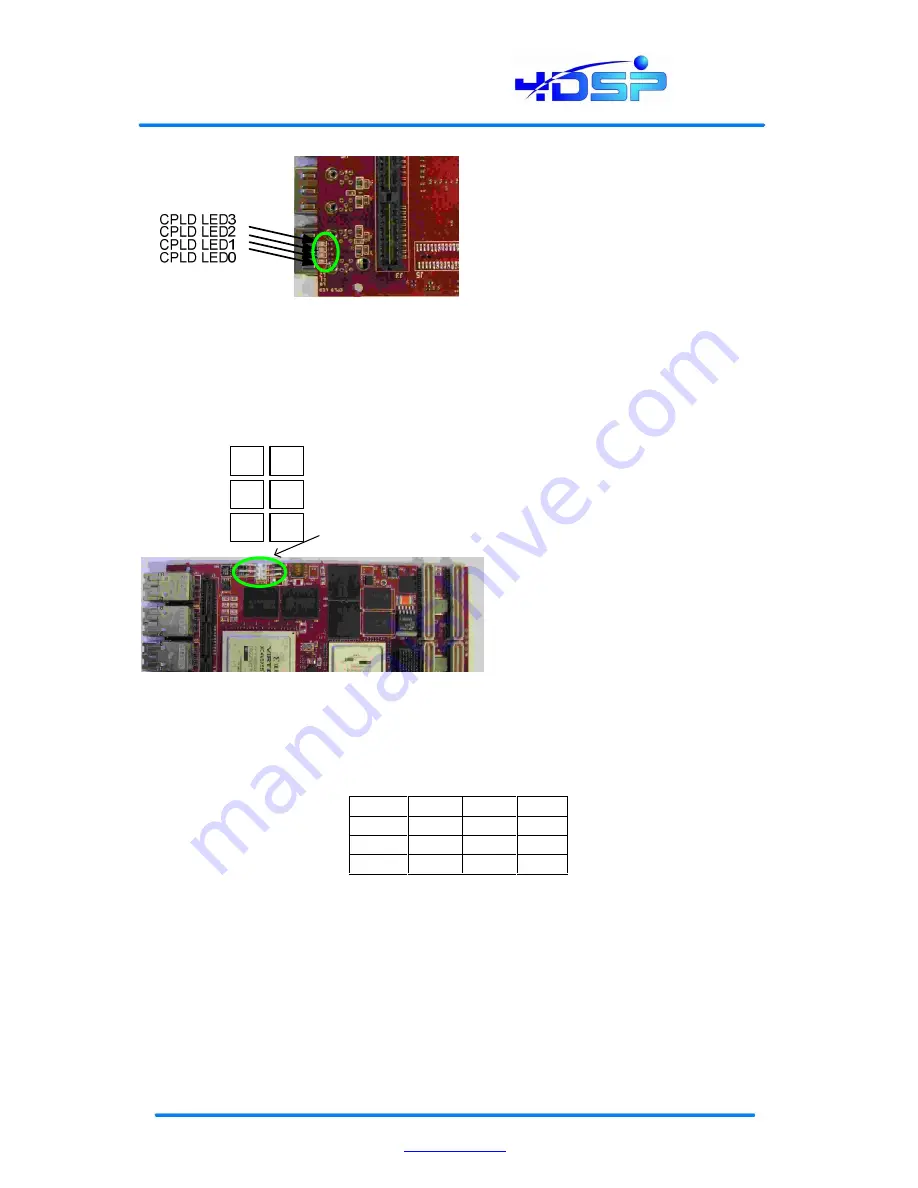
Figure 5: CPLD LED locations 


3.2.3  JTAG 

A JTAG connector is available on the AD484 for configuration purposes. The JTAG can also 
be used to debug the FPGA design with the Xilinx Chipscope. 

The JTAG connector is located on side 1 of the PCB in front  (see Figure 6). 

-7$*FRQQHFWRU

YFF

JQG

WFN

WPV

WGL

WGR


Figure 6: JTAG connector (J6) location 


The JTAG connector pinout is as follows: 


Pin # 

Signal  Signal 

Pin # 

1.8V 

TMS 

GND 

TDI 

TCK 

TDO 

Table 5 : JTAG pin assignment 

Содержание AD484

Страница 1: ...al 4DSP Inc 955 S Virginia Street Suite 214 Reno NV 89502 USA Email support 4dsp com This document is the property of 4DSP Inc and may not be copied nor communicated to a third party without the written permission of 4DSP Inc 4DSP Inc 2007 ...

Страница 2: ...nual V1 2 AD484 User manual February 2007 www 4dsp com 2 Revision History Date Revision Version 02 03 07 First release 1 0 03 29 07 Corrected typos 1 1 04 12 07 Added more details regarding clock synchronization 1 2 ...

Страница 3: ...nfiguration 10 3 2 1 Flash storage 10 3 2 2 CPLD device 10 3 2 3 JTAG 12 3 3 Clock tree 13 3 4 Memory resources 13 3 4 1 QDR2 SRAM 13 3 4 2 DDR2 SDRAM 13 3 5 A D inputs and outputs main characteristics 14 3 5 1 Analog inputs 15 3 5 2 Clock input and reference clock distribution 15 3 5 3 Multi module Synchronization 15 3 6 Front Panel optical transceivers 16 4 Power requirements 17 4 1 External pow...

Страница 4: ...w Voltage Differential Signaling MGT Multi Gigabit Transceiver MSB Most Significant Bit s PCB Printed Circuit Board PCI Peripheral Component Interconnect PCI e PCI Express PLL Phase Locked Loop PMC PCI Mezzanine Card QDR Quadruple Data rate SDRAM Synchronous Dynamic Random Access memory SRAM Synchronous Random Access memory Table 1 Glossary 1 2 Related Documents IEEE Std 1386 1 2001 IEEE Standard ...

Страница 5: ...tex 4 FPGAs Up to 4x 2 5Gbps optical transceivers for serial FPDP or gigabit Ethernet applications are available for communication with external systems The AD484 is mechanically and electrically compliant to the standard and specifications listed in section 1 2 of this document The AD484 implements a comprehensive clock circuitry that allows synchronisation among the converters and cascading modu...

Страница 6: ...the Xilinx PCI core in the Virtex 4 device A and an example VHDL design in the Virtex 4 device B so users can start digitizing and performing data manipulation right out of the box For more information about software installation and FPGA firmware please refer the AD484 Get Started Guide and to the Programmer s guide available online 3 Design 3 1 FPGA devices The Virtex 4 FPGA devices interface to...

Страница 7: ...ry The following performances have been recorded with the AD484 transferring data on the bus PCI X 64 bit 133MHz 750Mbytes s sustained PCI X 64 bit 66MHz 425Mbytes s sustained PCI 32 bit 33MHz 112Mbytes s sustained The PCI express 4 lane is using the MGT I Os on the Virtex 4 device A Power filtering low jitter clock and special routing are used to achieve the performances required by this standard...

Страница 8: ...O12 R8 P8 Pn4_IO13 14 15 Pn4_IO14 R6 R7 Pn4_IO15 16 17 Pn4_IO16 N21 M21 Pn4_IO17 18 19 Pn4_IO18 M20 M19 Pn4_IO19 20 21 Pn4_IO20 P19 N19 Pn4_IO21 22 23 Pn4_IO22 N18 N17 Pn4_IO23 24 25 Pn4_IO24 P16 N16 Pn4_IO25 26 27 Pn4_IO26 R18 P18 Pn4_IO27 28 29 Pn4_IO28 P21 P20 Pn4_IO29 30 31 Pn4_IO30 R17 R16 Pn4_IO31 32 33 Pn4_IO32 L9 M5 Pn4_IO33 34 35 Pn4_IO34 L5 AD11 Pn4_IO35 36 37 Pn4_IO36 AD10 L4 Pn4_IO37 3...

Страница 9: ...and is packaged in a 1148 ball Fineline Ball Grid array In terms of logic and dedicated DSP resources The FPGA B can be chosen in 5 different sizes SX55 LX40 LX60 LX80 LX100 and LX160 3 1 2 2 Virtex 4 device B external memory interfaces The Virtex 4 device B interfaces to four 8Mbytes QDR2 SRAM devices with 32 bit data bus Please note that the four QDR2 SRAM devices are only available with the LX8...

Страница 10: ... used to program and read the flash The data stored in the flash are transferred from the host motherboard via the PCI bus to the Virtex 4 device A and then to the CPLD that writes the required bit stream to the storage device A 31 25 MHz clock connects to the CPLD and is used to generate the configuration clock sent to the FPGA devices At power up if the CPLD detects that an FPGA configuration bi...

Страница 11: ...ut the board status Flashing FPGA A or B bitstream or user_ROM_register is currently being written to the flash ON FPGA A not configured LED 0 OFF FPGA A configured Flashing FPGA A or B bitstream or user_ROM_register is currently being written to the flash ON FPGA B not configured LED 1 OFF FPGA B configured Flashing The Virtex 4 device A has been configured with the safety configuration bitstream...

Страница 12: ...uration purposes The JTAG can also be used to debug the FPGA design with the Xilinx Chipscope The JTAG connector is located on side 1 of the PCB in front see Figure 6 7 FRQQHFWRU YFF JQG WFN WPV WGL WGR Figure 6 JTAG connector J6 location The JTAG connector pinout is as follows Pin Signal Signal Pin 1 1 8V TMS 4 2 GND TDI 5 3 TCK TDO 6 Table 5 JTAG pin assignment ...

Страница 13: ...ms and use the memory devices at different frequencies Both clock buffer devices CDM1804 and the frequency synthesizer ICS8430 61 are controlled by the Virtex 4 device A Figure 7 Clock tree 3 4 Memory resources 3 4 1 QDR2 SRAM Four independent QDR2 SRAM devices are connected to the Virtex 4 device B The QDR2 SRAM devices available on the AD484 are 2M words deep 8Mbytes per memory device Please not...

Страница 14: ...to peak AC coupled Input impedance 50 Ohm Termination implemented at the connector Frequency range 0 100MHz External Reference output Output voltage level 1 6 Volts peak to peak AC coupled Output impedance 50 Ohm Termination implemented at the connector External sampling clock input Input voltage level 0 5 3 3 Volts peak to peak AC coupled Input format Single ended or differential on option 3 3V L...

Страница 15: ...ctor on the front panel All samplings clocks are generated by the same chip It allows having them all synchronized to a single reference clock The on board clock uses the VCXO locked on an on board 10MHz reference The reference clock also can be external In that case the VCXO is still used It is also possible to input an external clock that is directly used to sample the analog signals In all case...

Страница 16: ...puts so multi rate applications can be implemented on the AD484 The MGT banks have power supplies independent from the digital supply provided to the FPGAs in order to insure low noise and data integrity The LT1963 device will be used to generate the 1 2V 1 5V and 2 5V necessary for the MGT to operate The power filtering network includes a 220nF decoupling capacitor and ferrite bead MP21608S221A p...

Страница 17: ...er For precise power measurements it is recommended to use the Xilinx power estimation tools for both FPGA A and B The maximum current rating given in the table below is the maximum current that can be drawn from each voltage rail in the case resources are used to their maximum level Device Interface Voltage Maximum current rating DCI and memory reference voltage 0 9V 5 A Virtex 4 device A B core ...

Страница 18: ...connectors It is used to power the board when it is in stand alone mode This is a right angled connector and it will be mounted on board only if the card is ordered in its stand alone version AD484 SA The height and placement of this connector on the PCB breaches the PMC specifications and the module should not be used in an enclosed chassis compliant to PMC specifications if the external power co...

Страница 19: ...ew 6 Environment 6 1 Temperature Operating temperature 0 C to 60 C Commercial 40 C to 85 C Industrial Storage temperature 40 C to 120 C 6 2 Convection cooling 600LFM minimum 6 3 Conduction cooling The AD484 can optionally be delivered as conduction cooled PMC The AD484 is compliant to ANSI VITA 20 2001 standard for conduction cooled PMC 7 Safety This module presents no hazard to the user ...

Страница 20: ... is not guaranteed unless it is installed within an adequate host system This module is protected from damage by fast voltage transients originating from outside the host system which may be introduced through the system 9 Warranty Hardware Software Firmware Basic Warranty included 1 Year from Date of Shipment 90 Days from Date of Shipment Extended Warranty optional 2 Years from Date of Shipment 1...

Отзывы: