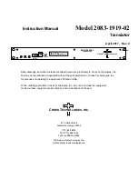
Summary of Contents for PSR-F50

Page 1: ...c Yamaha Corporation All rights reserved PDF 13 07 3 001894 CONTENTS SPECIFICATIONS 3 PANEL LAYOUT 3 CIRCUIT BOARD LAYOUT WIRING 4 DISASSEMBLY PROCEDURE 5 CIRCUIT BOARDS 11 TEST PROGRAM 17 PARTS LIST BLOCK DIAGRAM OVERALL CIRCUIT DIAGRAM 7 2 5 ...

Page 2: ...e therefore inevitable and changes in specification are subject to change without notice or obligation to retrofit Should any discrepancy appear to exist please contact the distribut s Service Division WARNING Static discharges can destroy expensive components Discharge any static electricity your body may have accumulated by grounding yourself to the ground bus in the unit heavy gauge black wires...

Page 3: ...V RU HTXLYDOHQW 3RZHU RQVXPSWLRQ KHQ XVLQJ 3 3RZHU GDSWRU XWR 3RZHU 2II XQFWLRQ HV QFOXGHG FFHVVRULHV 2ZQHUҋV 0DQXDO 3RZHU GDSWRU 3 RU HTXLYDOHQW 0D QRW EH LQFOXGHG GHSHQGLQJ RQ RXU SDUWLFXODU DUHD 3OHDVH FKHFN ZLWK RXU DPDKD GHDOHU 0XVLF 5HVW 2QOLQH 0HPEHU 3URGXFW 5HJLVWUDWLRQ 2SWLRQDO FFHVVRULHV 3RZHU GDSWRU 3 3 RU HTXLYDOHQW 6WHUHR HDGSKRQHV 3 PANEL LAYOUT 6WDQGE 2Q VZLWFK 0 67 5 92 80 EXWWRQV ...

Page 4: ...66 0 5 1 66 0 5 1 66 0 211 725 66 0 77 7KH SDUWV ZLWK µ LQ 3DUW 1R µ DUH QRW DYDLODEOH DV VSDUH SDUWV QVWDOODWLRQ 0DQXDO VROGHULQJ LS VROGHULQJ 5HG ZLUH LV DGMXVWHG WR 3LQ PDUN PDUN GJH PDUN LV DGMXVWHG WR 3LQ PDUN PDUN ODFN ZLUH LV FRQQHFWHG WR DWWHU 7HUPLQDO 5HG ZLUH LV FRQQHFWHG WR WHUPLQDO ODFN ZLUH LV FRQQHFWHG WR WHUPLQDO 5HG ZLUH LV FRQQHFWHG WR DWWHU 7HUPLQDO DXWLRQ H VXUH WR DWWDFK WKH UH...

Page 5: ...ked 70A and three 3 screws marked 80A Fig 1 RWWRP YLHZ 7RS YLHZ DWWHU FRYHU DVVHPEO HQWHU SDQHO DVVHPEO 6LGH SDQHO DVVHPEO 5 6LGH SDQHO DVVHPEO 1 2 Release the two 2 hooks marked A The center panel assembly can then be removed Fig 1 Caution Be sure to attach the removed filament tape just as it was before removal Fig 1 ...

Page 6: ... 2 1 Remove the center panel assembly See procedure 1 2 2 Remove the following screws Each circuit board can then be removed Fig 2 Table 1 7RS YLHZ 6 31 0 0 Fig 2 Table 1 LUFXLW RDUG 6FUHZ 5HI 1R 47 LJ 0 LUFXLW RDUG 0 LUFXLW RDUG 31 LUFXLW RDUG 6 LUFXLW RDUG ...

Page 7: ...an then be removed Fig 1 The side panel assembly L and R can be removed in the same manner 4 Speaker L R Time required About 5 minutes 4 1 Remove the center panel assembly See procedure 1 4 2 Remove the side panel assembly See procedure 3 4 3 Remove the four 4 screws marked 40 The speaker can then be removed Fig 3 The speaker L and R can be removed in the same manner RWWRP YLHZ 6SHDNHU 6LGH 3DQHO ...

Page 8: ...tegrated in a set Fig 4 5 3 2 To remove a set remove the two 2 each screws marked 110A The white and black keys in the set can then be removed Fig 4 When removing unfasten the two 2 hooks at the back of the black keys upward and lift the white and black keys while pulling them toward you a little Photo 1 5 3 3 To remove the white key C6 remove the screw marked 110B unhook as described in Procedure...

Page 9: ...ard 5 5 1 Remove the white and black keys from C1 to B3 See Fig 4 and Procedure 5 3 5 5 2 Remove the twelve 12 screws marked 90A The 61L circuit board can then be removed Fig 5 5 6 61H Circuit Board 5 6 1 Remove the white and black keys from C4 to C6 See Fig 4 and Procedure 5 3 5 6 2 Remove the eight 8 screws marked 90B The 61H circuit board can then be removed Fig 5 7RS YLHZ 5XEEHU FRQWDFW 5XEEHU...

Page 10: ...embly Fig 1 6 1 4 Lift the spring terminal A a little and slide it in the upper right direction to remove it Fig 6 6 1 5 Remove the hook for the spring terminal B to pull it out from inside Fig 6 6 2 Spring Terminal C and Spring Terminal D Time required About 1 minute each 6 2 1 Remove the battery cover assembly See procedure 6 1 5 6 2 2 Remove the hooks to pull out the spring terminal C and sprin...

Page 11: ...ard YF156C0 12 7SEG Circuit Board YF156C0 12 61H Circuit Board XT701C0 14 61L Circuit Board YE761A0 15 CIRCUIT BOARDS AM Circuit Board Note See parts list for details of circuit board component parts 2NA ZF28700 2 WR 77 5 6 WR 63 5 WR 63 5 5 WR 0 1 3 21 6 287387 1 9 Component Side ...

Page 12: ...12 PSR F50 PN Circuit Board 7SEG Circuit Board Component Side Component Side WR 6 1 WR 0 1 2NA ZF28700 2 WR 31 1 ...

Page 13: ...13 PSR F50 Component Side DM Circuit Board WR 31 1 WR 0 1 WR 1 WR 1 Pattern Side 2NA ZF28690 1 ...

Page 14: ...14 PSR F50 61H Circuit Board WR 0 1 ҋ ҋ Component Side 2NAK8 ZF61670 1 ...

Page 15: ...15 PSR F50 61L Circuit Board Component Side 2NAK8 ZD49640 ҋ WR 0 1 ҋ ҋ ҋ ...

Page 16: ... VXSSO IRU 0 LUFXLW RDUG 9 SRZHU IRU GLJLWDO FLUFXLW 9 SRZHU IRU GLJLWDO FLUFXLW 9 SRZHU IRU FLUFXLW 38 UHVHW VLJQDO XGJPHQW FULWHULD 0RUH WKDQ 9 9 9 9 9 9 9 9 9 0HDVXUHG E 0XOWLPHWHU 0XOWLPHWHU 0XOWLPHWHU 0XOWLPHWHU 0XOWLPHWHU 0HDVXUHG 1 1 1 1 1 1 3DUWV ZLWK SRVVLEOH GHIHFWV 7 RU 75 2Q 0 LUFXLW RDUG 8VH WKH VWDQGDUG DGDSWHU 3 RU 3 IRU FKHFN RSHUDWLRQ 7KHUH DUH QRW DYDLODEOH DV VSDUH SDUWV 7KH H F...

Page 17: ...While holding down the keys C 3 F3 and G 3 simultaneously press the STANDBY ON switch Executed sequentially from 1 to 7 of auto mode test item 3 Test procedure Manual mode 1 When the test program is started TST will be displayed on the 7 segment LED 2 Press the Tenkey or Tenkey button to select a test program item 3 Press the START STOP button to execute the test If the result is OK or test item i...

Page 18: ...ess the SONG STYLE button or the lowest key white key C1 to return to the item selection display 24 T24 Confirm that all LEDs turned on 5 45 T45 Insert the plug of the AC adapter into a DC IN 12V jack 7 Confirm that PAS is displayed on the 7 segment LED 55 T55 Checks the ROM connected to the CPU bus Full address Confirm that PAS is displayed on the 7 segment LED It will take about 10 seconds for t...

Page 19: ...S02 S03 S04 S05 S06 S07 S08 S09 S10 S11 S12 S13 S14 S15 S16 S17 S18 S19 S20 S21 63 127 621 67 92 0 67 5 92 80 7 032 7 3 7HQNH 7HQNH 7HQNH 7HQNH 7HQNH 7HQNH 0 67 5 92 80 087 7HQNH 7HQNH 7HQNH 7HQNH 7HQNH 7HQNH 81 7 21 3 86 872 67 57 6723 6 7 1 0 ...

Page 20: ...s QTY show quantities for each unit The parts with in PART NO are not available as spare parts This mark in the REMARKS column means these parts are interchangeable The second letter of the shaded part number is O not zero The second letter of the shaded part number is I not one PARTS LIST CONTENTS OVERALL ASSEMBLY 2 KEYBOARD ASSEMBLY 16NS 4 ELECTRICAL PARTS 5 ...

Page 21: ...PSR F50 2 OVERALL ASSEMBLY D F E 65 65 65 6 6 65 6 6 6 6 65 65 65 H ERDUG DVVHPEO 6HH SDJH HQWHU SDQHO DVVHPEO 6LGH SDQHO DVVHPEO 6LGH SDQHO 5 DVVHPEO RZHU FDVH DVVHPEO ...

Page 22: ...HM 3W ス ピ ー カ SR30 WIRING ASSEMBLY SP 2P L 525 S P 線 材 ZF94030 SR40 WE97460R BIND HEAD TAPPING SCREW B 4 0X8 MFZN2W3 B タ イ ト B I N D 4 01 SR60 CUSHION PE 275X8X1 ク ッ シ ョ ン P E WT44070 SR70 NONWOVEN CLOTH 10X8X0 5 不 織 布 WK60830 SR80 CUSHION PE 145X6X1 ク ッ シ ョ ン P E ZH99880 SIDE PANEL L ASSEMBLY PK PSR F50 左 パ ネ ル A s s y ZF61340 SL10 ZF610400 SIDE PANEL L MOLDING サ イ ド パ ネ ル L 成 形 品 SL20 YF173A00 L...

Page 23: ...CONTACT 16N 1M 16N OCT 1M 接 点 ゴ ム 5 50 WE152500 RUBBER CONTACT 16N 1M OCT LIM 接 点 ゴ ム 5 03 60 VZ271900 RUBBER CONTACT 16N 1M C 16N C_ 1M 接 点 ゴ ム 04 70 VZ303020 FELT L 11x827 WHITE 827 11 SHIRO フ ェ ル ト L 75 VZ302901 FELT U836 836 5 SHIRO フ ェ ル ト U 02 90 WE774300 BIND HEAD B TIGHT SCREW 3 0X8 MFZN2W3 B タ イ ト B I N D 20 110 WF49200R BIND HEAD TAPPING SCREW P 3 0X20 MFZN2W3 P タ イ ト B I N D 11 01 120 Z...

Page 24: ... 3 3V I C REGULATOR 3 3V ZF836100 CIRCUIT BOARD AM A M シ ー ト ZF28700 YF156C0 ZF836200 CIRCUIT BOARD PN P N シ ー ト ZF28700 YF156C0 ZF836300 CIRCUIT BOARD 7SEG 7 S E G シ ー ト ZF28700 YF156C0 IC151 YF011A00 IC ANALOG AMP TA8227AP 2 5W 2CH ア ン プ I C POWER AMP 2 5W 2CH JK101 WZ704401 POWER JACK DC 502 AG PBT 2 0 電 源 コ ネ ク タ DC IN JK151 ZA590000 PHONE JACK MINI STEREO ホ ー ン コ ネ ク タ PHONES OUTPUT ZD496300 ...

Page 25: ...5W X 2 TA8227AP KIN1 6 KIN1 6 KB1 11 KB1 7 KB7 11 KB1 8 LPF Driver Driver 48 51 PORTB1 4 DIGIT 0 2 PD1 8 PORTE0 52 3 3D RESET 4 2V 54ms SWLL Internal Clock 33 8688MHz Master Clock 67 7376MHz 3 3L 3 3D Internal 1 8V REGULATOR 7seg_e0 2 7seg_lat 5D PSW PSW V B SW MATRIX SW 21PCS VOLUME is included PHONES OUTPUT 5V REGULATOR 5D 3 3V REGULATOR 3 3D Over Current Protection 3 3V REGULATOR 61L 61H PN 7SE...

Page 26: ...RALL CIRCUIT DIAGRAM 1 3 DM PSR F50 Page 2 PSR F50 PSR F50 to I10 from G6 to PN CN201 Page3 P5 to AM CN103 Page3 P11 to 61L CN1 Page4 M10 to 61H CN1 Page4 M4 REGULATOR 3 3V REGULATOR 3 3V REGULATOR 5V CPU SWLL FLASH ROM 16M VOLTAGE DETECTOR D FF OP AMP 28CC1 2001119320 3 DM ...

Page 27: ...A 12 11 10 9 8 7 6 5 4 3 2 1 PSR F50 PSR F50 PSR F50 OVERALL CIRCUIT DIAGRAM 2 3 AM PN 7SEG PSR F50 Page 3 to DM CN301 Page2 B9 to DM CN1 Page2 N4 POWER AMP 2 5W 2CH 28CC1 2001119321 3 28CC1 2001119321 3 28CC1 2001119321 3 PN AM 7SEG ...

Page 28: ... 4 3 2 1 PSR F50 OVERALL CIRCUIT DIAGRAM 3 3 61H 61L PSR F50 Page 4 PSR F50 PSR F50 to DM CN201 Page2 N11 to DM CN202 Page2 N7 B7 B6 B5 B4 B3 B2 B1 N12 N11 N16 N15 N14 N13 N16 N15 N14 N13 N12 N11 B11 B10 B9 B8 B7 28CC1 2001113059 28CC1 2001113060 61H 61L ...

Reviews: