background image

SERVICE MANUAL

PK

001627

HAMAMATSU, JAPAN

 CONTENTS

SPECIFICATIONS

.............................................. 3/4
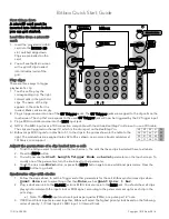
PANEL LAYOUT

...................................... 5

PSR-740 BLOCK DIAGRAM

.... 6

PSR-640 BLOCK DIAGRAM

.... 7

CIRCUIT BOARD LAYOUT

................. 8

DISASSEMBLY PROCEDURE

............................. 10

LSI PIN DESCRIPTION

............................... 14

IC BLOCK DIAGRAM

.................................. 19

CIRCUIT BOARDS

........................................ 20

TEST PROGRAM

............................. 25/27

DATA INITIALIZATION

.......................................... 29

ALERT MESSAGE LIST

................... 30/32

MIDI DATA FORMAT

................. 34

PSR-740 MIDI IMPLEMENTATION CHART ......................... 49
PSR-640 MIDI IMPLEMENTATION CHART ......................... 50
PARTS LIST
OVERALL CIRCUIT DIAGRAM

PSR-740

PSR-640

PSR-740 19990901-160000
PSR-640 19990901-120000

  1.82K-9201  

  Printed in Japan ‘99.08

Содержание PortaTone PSR-740

Страница 1: ... PROCEDURE 10 LSI PIN DESCRIPTION 14 IC BLOCK DIAGRAM 19 CIRCUIT BOARDS 20 TEST PROGRAM 25 27 DATA INITIALIZATION 29 ALERT MESSAGE LIST 30 32 MIDI DATA FORMAT 34 PSR 740 MIDI IMPLEMENTATION CHART 49 PSR 640 MIDI IMPLEMENTATION CHART 50 PARTS LIST OVERALL CIRCUIT DIAGRAM PSR 740 PSR 640 PSR 740 19990901 160000 PSR 640 19990901 120000 1 82K 9201 Printed in Japan 99 08 ...

Страница 2: ...4 35 234 134 77 76 222 225 86 98 99 102 103 223 221 81 101 135 136 IC6 IC4 IC14 IC14 IC7 IC8 IC15 IC11 IC12 IC9 IC310 IC320 IC210 220 IC510 IC410 IC610 IC710 IC13 IC14 IC15 11 13 32 14 29 28 13 14 29 28 13 IC10 IC19 IC18 IC20 IC21 IC16 IC17 IC5 IC1 IC2 PC1 19 6 17 11 11 TA2 TA1 13 14 27 28 29 17 19 21 5 7 1 11 13 32 22 24 29 10 13 14 37 1 3 5 7 20 21 40 4 39 4 15 14 13 12 11 2 2 1 ...

Страница 3: ... IC610 IC710 IC1 PC1 IC360 IC360 IC350 IC330 IC300 IC320 IC310 IC510 TR501 505 IC530 IC500 11 IC430 IC420 IC410 IC400 IC800 19 6 17 10 13 14 37 1 3 5 7 20 21 40 4 39 11 13 14 31 30 22 24 29 11 13 32 2 11 13 32 1 4 15 14 13 12 11 25 158 159 163 164 IC210 12 74 73 43 44 101 IC 220 IC100 108 194 196 43 48 53 114 11 6 10 9 150 151 152 122 IRQFD ...

Страница 4: ...O 109 DREQ0 PE0 I O DMA transfer request Port E 38 A19 O Address bus 110 TIOC0B PE1 I O MTU input capture output compare ch 0 Port E 39 A20 O 111 DREQ1 PE2 I O DMA transfer request Port E 40 VCC I Power supply 112 VCC I Power supply 41 A21 O Address bus 113 PE3 I O 42 VSS I Ground 114 PE4 I O Port E 43 RD O Read 115 PE5 I O 44 WDTOVF O Watch dog timer overflow 116 PE6 I O 45 D31 I O Data bus 117 V...

Страница 5: ...8 SMD7 I O Wave memory data bus 122 CMD15 I O Program memory Data bus 39 SMD0 I O Wave memory data bus 123 CMD0 I O Program memory Data bus 40 SMD15 I O Wave memory data bus 124 CMA21 O Program address bus 41 SOE O read signal 125 PDT15 I O 42 SWE O write signal 126 PDT14 I O 43 SRAS O RAS signal 127 PDT13 I O 44 SCAS O CAS signal 128 PDT12 I O 45 REFRESH O REFRESH signal 129 PDT11 I O SWX access ...

Страница 6: ... 129 130 131 132 133 134 135 136 137 138 139 140 141 142 143 144 145 146 147 148 149 150 151 152 153 154 155 156 157 158 159 160 161 162 163 164 165 166 167 168 169 170 171 172 173 174 175 176 177 178 179 180 181 182 183 184 185 186 187 188 189 190 191 192 193 194 195 196 197 198 199 200 201 202 203 204 205 206 207 208 209 210 211 212 213 214 215 216 217 218 219 220 221 222 223 224 225 226 227 228...

Страница 7: ...N PIN NO 81 82 83 84 85 86 87 88 89 90 91 92 93 94 95 96 97 98 99 100 101 102 103 104 105 106 107 108 109 110 111 112 113 114 115 116 117 118 119 120 121 122 123 124 125 126 127 128 129 130 131 132 133 134 135 136 137 138 139 140 141 142 143 144 145 146 147 148 149 150 151 152 153 154 155 156 157 158 159 160 I O O O O O O O O O O O O I O O I I I O O O O O O I O I I I I I I I I I I I I I I O I O I ...

Страница 8: ...l data input 14 B2 I O 34 D5 CK O Clock for serial operation 15 B3 I O Port B 35 D6 INT2 I Interrupt request 2 16 B4 I O 36 STBY I Standby mode signal 17 B5 I O 37 TIMER I Timer 18 B6 I O 38 XTAL O Clock 19 B7 I O 39 EXTAL I 20 VSS Ground 40 VCC Power supply PIN NAME I O FUNCTION NO PIN NAME I O FUNCTION NO HD63B05V0F073P XR951A00 CPU PIN NAME I O FUNCTION NO PIN NAME I O FUNCTION NO AK5351 VF E2 ...

Страница 9: ... 12 13 14 15 16 17 18 19 20 21 22 23 24 25 26 27 28 29 30 31 32 I O I I I I I I I I I I O I O I O I O I O I O I O I O O O I I I I I I I I 8 5 XTALSET RESET E RD RW WR CS DACK RS0 RS1 VSS1 VSS2 D0 D1 D2 D3 D4 D5 D6 D7 DREQ IRQ DEND VSS3 1 2 EX1 VCC1 NUM1 NUM3 IFS SFORM INP READY WPRT NAME Data transmission speed Clock select Rest Enable Read Read write Write Chip select DMA acknowledge Register sel...

Страница 10: ...AM LIST 1 001 Version DisplaysROMversion ROM Program Wave versions are displayed alternately on the LCD 2 002 Rom Chk1 Checks the ROM The test results appear on the LCD 3 003 Ram Chk1 Checks all the RAMs that are connected to the CPU The test results appear on the LCD 4 004 WaveRomChk1 Checks the WAVE ROMs that are connected to the CPU The test results appear on the LCD 7 007 FDD Chk Insert the fl...

Страница 11: ...utputwhenrotatingittomaximum 35 035 EXP Pedal Chk Connect the expression pedal FC 7 to the FOOT VOLUME jack Check that the C3 note is output and the LCD displays 0 when pressing the expression pedal to the lowered position and the C4 note is output and the LCD displays 127 when backing it to the raised position 37 037 Midi Chk After connecting the MIDI IN jack and MIDI OUT jack with a MIDI cable e...

Страница 12: ...rrying out the data initialization procedure will usually restore normal operation if the PSR 740 640 freezes or begins to act erratically for any reason All data can be initialized and restored to the factory preset condition by turning on the power while holding the highest rightmost white key on the keyboard Now initializing the internal memory willappearbrieflyonthedisplay DATA INITIALIZATION ...

Страница 13: ...damage both the disk and the drive The disk s memory capacity is full and no additional data can be recorded Delete one or more unneeded songs using Delete and attempt the operation again When using the Copy operation the inserted disk is different from the source or destination disk Remove the disk and re insert the proper Disk More than one file has the same name on the disk Change the name Maxi...

Страница 14: ...ion in the Multi Pad Recording mode The backup data is faulty Use the data initialization function All data can be initialized and restore to the factory preset condition by turning the STANDBY switch ON while holding the highest rightmost white key on the keyboard This message may appear when the Host Select switch is set appropriately and the serial cable is connected to the TO HOST but not to t...

Страница 15: ... CN310 to MIC JACK CN5 to PN1 CN1 N C to PN1 CN2 CPU FDC SRAM 1M DECODER INVETER EPROM MAIN1 32M EPROM MAIN2 32M OR OR OR OR AND AND D FF DECODER D FF TRANSISTOR ARRAY TRANSISTOR ARRAY TRANSISTOR ARRAY SRAM 256K LCDC INVERTER INVERTER DRAM 4M DRAM 4M FDC REGULATOR 9V REGULATOR 5V DC DC CONVERTER 1 2 28CC1 8812655 28CC1 8811360 28CC1 8811360 2NA 8814265 28CC1 8814267 Note See parts list for details...

Страница 16: ...IC MIC JACK SWP30B VOP3 INVERTER INVERTER WAVE ROM LL 32M WAVE ROM HL 32M WAVE ROM LH 16M WAVE ROM HH 16M REGULATOR 3 3V DRAM 4M DRAM 4M ADC DAC OP AMP OP AMP 2 2 LED DRIVER 0P AMP 0P AMP MIC LINE IN 28CC1 8814267 28CC1 8814268 28CC1 8814266 not installed installed RE GR Note See parts list for details of circuit board component parts Ceramic Capacitor Semi Conductive Ceramic Capacitor 560P 4 7K 5...

Страница 17: ...PN1 CN2 to PN1 CN1 CPU RESET DECODER SRAM 1M PROGRAM1 ROM H 32M PROGRAM2 ROM L32M DRAM 16M DECODER DECODER D FF DECODER TRANSISTOR ARRAY TRANSISTOR ARRAY OR AND AND D FF SRAM 256K LCDC INVERTER INVERTER DC DC CONVERTER FDC REGULATOR 5V DAC ROM WAVE1 32M ROM WAVE2 32M SWX00B REGULATOR 3 3V DRAM 4M to Back light Assembly 28CC1 8812655 28CC1 8811360 28CC1 8811360 28CC1 8813199 2NA 8814265 Note See pa...

Страница 18: ...acitor REGULATOR 9V POWER AMP 0 65W 2CH POWER AMP 1 7W OP AMP OP AMP EQUALIZER EQUALIZER INVERTER LINE TRANSCEIVER PSR 640 PSR 740 HELP DIRECT ACCESS LANGUAGE COUNT INTRO INTRO MAIN AUTO FILL SIMPLE ENDING ON OFF REGISTRATION MEMORY MULTI PAD ONETOUCH SETTING UTILITY DISK 1 2 3 4 5 6 7 8 9 NO YES 0 SONG PSR 640 39K PSR 740 470K R503 R504 2 2K 1 8K R603 R604 LA4525 28CC1 8813198 28CC1 8813198 28CC1...

Отзывы: