Toshiba MD20FL3, Service Manual
The Toshiba MD20FL3 is a versatile and efficient product, designed to meet all your entertainment needs. For detailed instructions and troubleshooting, make sure to download the free Service Manual from manualshive.com. This manual provides comprehensive information on operating, maintaining, and troubleshooting the MD20FL3, ensuring optimal performance and longevity.
Share
Download


Reviews:
No comments
Related manuals for MD20FL3
HLC24XSL2
Brand: Haier Pages: 28

CL32Z40DSK
Brand: Samsung Pages: 36

CL28A20HE
Brand: Samsung Pages: 80

MS3250C
Brand: Magnavox Pages: 40
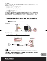
Medi TV
Brand: Packard Bell Pages: 48

DTQ-19V6FCB
Brand: Daewoo Pages: 29

LED49D2900S
Brand: TCL Pages: 32

L42V6300F3DE
Brand: TCL Pages: 16

SE55FGT
Brand: Seiki Pages: 28

82V42UHD
Brand: Vidao Pages: 40

AB-LED32L32D 3D
Brand: CRISTOR Pages: 18

CSL1505
Brand: Symphonic Pages: 4

L19A11E
Brand: TCL Pages: 17

LE24D3140_30
Brand: AOC Pages: 64

JCTV3245XA
Brand: Citizen Pages: 28

Vision 20 LCD 51-8610 Top
Brand: Grundig Pages: 38

S7311
Brand: ricoo Pages: 12

L-GL600
Brand: GEM Pages: 1


