


User's Guide
SBAU233A – October 2014 – Revised November 2015
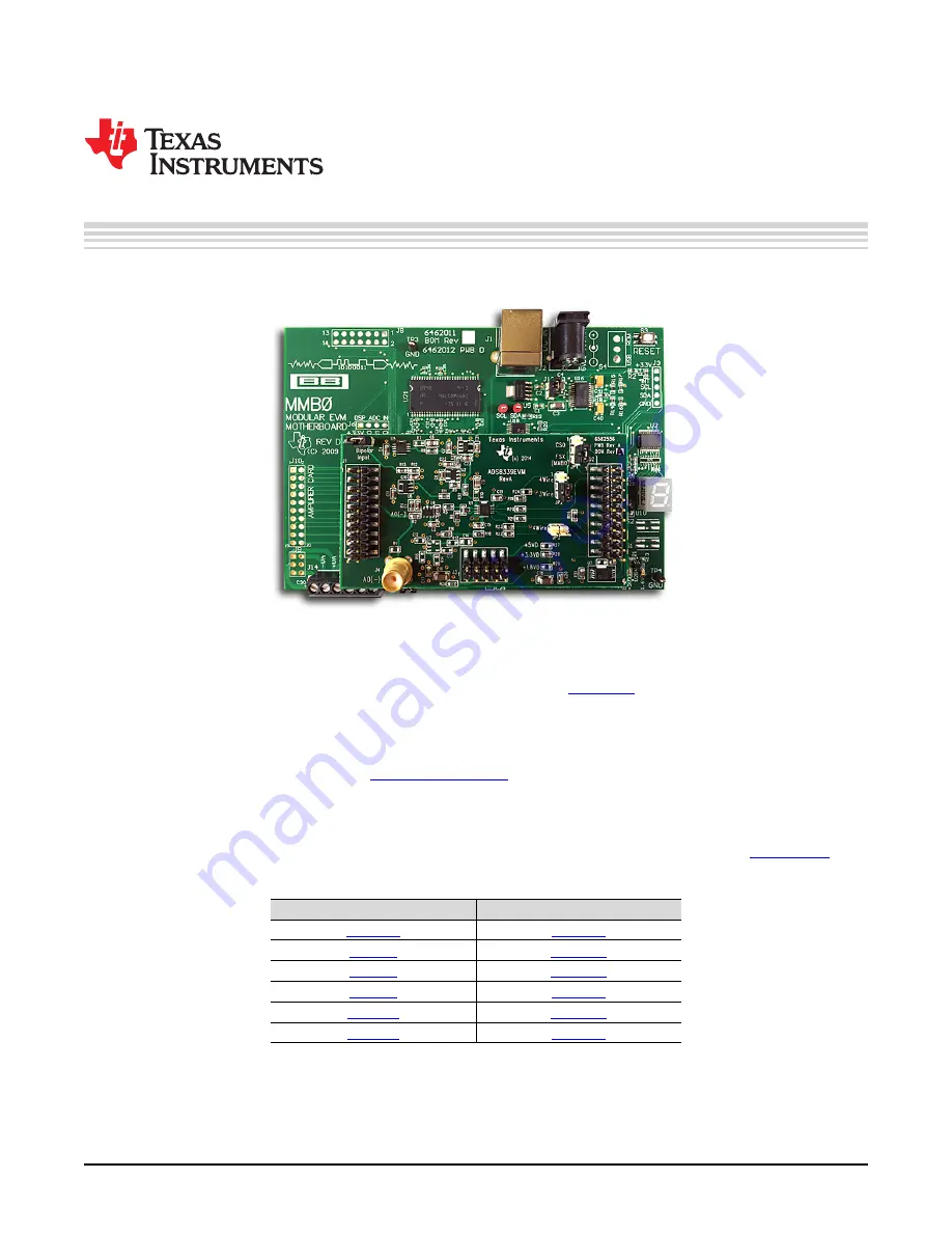
ADS8339EVM-PDK
ADS8339EVM-PDK
This user's guide describes the operation and use of the
evaluation module (EVM). The
ADS8339 is a 16-bit, pseudo-differential, unipolar, successive approximation register (SAR), analog-to-
digital converter (ADC) with a maximum throughput of 250-KSPS. The device is a very low-power ADC
with excellent noise and distortion performance for ac or dc signals. The performance demonstration kit
(PDK) eases EVM evaluation with additional hardware and software for computer connectivity through a
universal serial bus (USB). The
includes the ADS8339EVM as a daughter card,
MMB0 motherboard, and an A-to-B USB cable. This user's guide covers circuit description, schematic
diagram, and bill of materials for the ADS8339EVM daughter card. Throughout this document, the
abbreviation EVM and the term evaluation module are synonymous with the ADS8339EVM-PDK.
The following related documents are available through the Texas Instruments web site at
Related Documentation
Device
Literature Number
ADCPro is a trademark of Texas Instruments.
Windows is a registered trademark of Microsoft Corporation.
SPI is a trademark of Motorola, Inc.
Samtec is a trademark of Samtec, Inc.
All other trademarks are the property of their respective owners.
1
SBAU233A – October 2014 – Revised November 2015
ADS8339EVM-PDK
Copyright © 2014–2015, Texas Instruments Incorporated


