background image

®

  SUPER P4DPL-8GM
  SUPER P4DPL-iGM
  SUPER P4DPL-M

USER’S MANUAL

   Revision 1.0


S

UPER

Summary of Contents for SUPER P4DPL-8GM

Page 1: ...SUPER P4DPL 8GM SUPER P4DPL iGM SUPER P4DPL M USER S MANUAL Revision 1 0 SUPER...

Page 2: ...ILITY TO USE THIS PRODUCT OR DOCUMENTATION EVEN IF ADVISED OF THE POSSIBILITY OF SUCH DAMAGES IN PARTICULAR THE VENDOR SHALL NOT HAVE LIABILITY FOR ANY HARDWARE SOFTWARE OR DATA STORED OR USED WITH TH...

Page 3: ...h instructions on handling static sensitive devices Read this chapter when you want to install the processor and memory modules and when mounting the mainboard in the chassis Also refer to this chapte...

Page 4: ...1 10 Intel E7500 Chipset System Block Diagram 1 12 1 2 Chipset Overview 1 13 1 3 Special Features 1 13 ATI Graphics Controller 1 13 BIOS Recovery 1 13 Recovery from AC Power Loss 1 14 1 4 PC Health M...

Page 5: ...12 Keylock 2 13 Wake On LAN 2 13 Wake On Ring 2 13 2 6 Jumper Settings 2 14 Explanation of Jumpers 2 14 CMOS Clear 2 14 Mb LAN Enable Disable 2 15 Gb LAN Enable Disable 2 15 VGA Enable Disable 2 15 P...

Page 6: ...guration 3 2 3 2 Technical Support Procedures 3 2 3 3 Frequently Asked Questions 3 3 3 4 Returning Merchandise for Service 3 5 Chapter 4 PhoenixBIOS 4 1 Introduction 4 1 4 2 Running Setup 4 2 4 3 Main...

Page 7: ...following items have all been included with your motherboard If anything listed here is damaged or missing contact your retailer One 1 Supermicro Mainboard One 1 ribbon cable for IDE devices One 1 flo...

Page 8: ...com Europe Address SuperMicro Computer B V Het Sterrenbeeld 28 5215 ML s Hertogenbosch The Netherlands Tel 31 0 73 6400390 Fax 31 0 73 6416525 Email sales supermicro nl General Information support sup...

Page 9: ...Chapter 1 Introduction 1 3 Introduction Notes...

Page 10: ...SUPER P4DPL 8GM P4DPL iGM P4DPL M User s Manual 1 4 Introduction Figure 1 1 SUPER P4DPL 8GM P4DPL iGM Image...

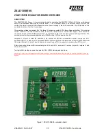
Page 11: ...Chapter 1 Introduction 1 5 Introduction Figure 1 2 SUPER P4DPL M Image...

Page 12: ...XL J29 Chassis Fan3 CPU 2 CPU 1 ICH3 AIC 7902 Battery Speaker COM2 33 MHz PCI 2 33 MHz PCI 1 33 MHz PCI 3 133 MHz PCI X 6 66 MHz PCI X 5 66 MHz PCI X 4 J12 IR CIR WD PWRLED SPKR BIOS WOL J35 JBT1 JD1...

Page 13: ...Gb LAN Gb LAN Ethernet Port IDE 1 IDE 2 IDE 1 2 Hard Disk Drive Connectors FPUSB0 1 Front Side USB0 1 Headers J9 PS 2 Keyboard Mouse Ports J15 Processor Power Connector J29 Parallel Printer Port JA1 U...

Page 14: ...CONN DIMM 3A Parallel Port VGA COM1 USB0 1 Keyboard Mouse Mb LAN MCH Rage XL J29 Chassis Fan3 CPU 2 CPU 1 ICH3 Battery Speaker COM2 33 MHz PCI 2 33 MHz PCI 1 33 MHz PCI 3 133 MHz PCI X 6 66 MHz PCI X...

Page 15: ...ry RAM Slots COM1 COM2 COM1 COM2 Serial Port Connector CPU Chassis FAN CPU Chassis Fan Headers IDE 1 IDE 2 IDE 1 2 Hard Disk Drive Connectors FPUSB0 1 Front Side USB0 1 Headers J9 PS 2 Keyboard Mouse...

Page 16: ...ted but will only run at 200 MHz See Section 2 3 for details Chipset Intel E7500 Plumas chipset Expansion Slots One 64 bit 133 MHz PCI X Two 64 bit 100 MHz PCI X Three 32 bit 33 MHz PCI BIOS 4 Mb Phoe...

Page 17: ...M 2 EIDE Ultra DMA 100 bus master interfaces 1 floppy port interface up to 2 88 MB 2 Fast UART 16550A compatible serial ports 1 EPP ECP Parallel Port Enhanced Parallel Port Extended Capabilities Port...

Page 18: ...h motherboard Because the P4DPL iGM and P4DPL M have no onboard SCSI controller PCI X slots 4 and 5 run on a 100 MHz PCI X bus MCH 400 MHz Host Bus 200 MHz Memory Bus P64H2 Processor Processor DDR 200...

Page 19: ...P64H2 interface is a 1 GB s point to point connection using a 16 bit wide 66 MHz base clock at a 8x data transfer rate The ICH3 I O Controller Hub provides various integrated functions including a two...

Page 20: ...oltages continuously Once a voltage becomes unstable a warning is given or an error message is sent to the screen Users can adjust the voltage thresholds to define the sensitivity of the voltage monit...

Page 21: ...ard drive space for saving the data you can be alerted of the potential problem Auto Switching Voltage Regulator for the CPU Core The auto switching voltage regulator for the CPU core can support up t...

Page 22: ...t blinking to indicate that the CPU is in suspend mode When the user presses any key the CPU will wake up and the LED will automatically stop blinking and remain on Main Switch Override Mechanism When...

Page 23: ...t power supplies generally meet the specifications required by the CPU some are inadequate You should use one that will supply at least 400W of power and includes the additional 12V 8 pin power connec...

Page 24: ...byte send receive FIFO a programmable baud rate generator complete modem control capability and a processor interrupt system Each UART includes a 16 byte send receive FIFO a programmable baud rate ge...

Page 25: ...emoving the board from the anti static bag Handle the board by its edges only do not touch its components periph eral chips memory modules or gold contacts When handling chips or modules avoid touchin...

Page 26: ...es as shown on right White pegs 4 2 Insert the white pegs into the black anchors Do not force the white pegs all the way in only about 1 3 of the way into the black anchors 3 Place a retention bracket...

Page 27: ...PU socket 2 is auto matically disabled if only one CPU is used Pin 1 7 Press the lever down until you hear it click into the locked position Socket lever in locked position 4 Secure the other retentio...

Page 28: ...d the chassis match Although a chassis may have both plastic and metal mounting fasteners metal ones are highly recommended because they ground the motherboard to the chassis Make sure the metal stand...

Page 29: ...IMM Installation See Figure 2 2 1 Insert the desired number of DIMMs into the memory slots starting with Bank 1 The memory scheme is interleaved so you must install two modules at a time beginning wit...

Page 30: ...I O ports are color coded in conformance with the PC 99 specification See Figure 2 3 below for the colors and locations of the various I O ports Figure 2 3 I O Port Locations and Definitions Mouse Gre...

Page 31: ...d especially for use with Supermicro server chassis See Figure 2 4 for the descriptions of the various control panel buttons and LED indicators Refer to the following section for descriptions and pin...

Page 32: ...erset ATX 24 pin specification however it also supports a 20 pin power supply connector Make sure that the ori entation of the PS connector is correct Pins 1 thru 4 5 thru 8 Definition Ground 12v Proc...

Page 33: ...e NIC1 Network Interface Con troller LED connection is located on pins 11 and 12 of JF2 Attach the NIC1 LED cable to display net work activity Refer to the table on the right for pin definitions HDD L...

Page 34: ...ial Bus USB0 1 Two Universal Serial Bus ports are located beside the PS 2 key board mouse ports USB0 is the bottom connector and USB1 is the top connector See the table on the right for pin definition...

Page 35: ...on the right for pin definitions The mouse port is above the keyboard port See Fig ure 2 3 PS 2 Keyboard and Mouse Port Pin Definitions J9 Pin Number 1 2 3 4 5 6 Definition Data NC Ground VCC Clock NC...

Page 36: ...he speaker connection See the table on the right for speaker pin definitions Note The speaker connector pins are for use with an external speaker If you wish to use the onboard speaker you should clos...

Page 37: ...onnector and cable Wake On Ring The Wake On Ring header is des ignated JWOR1 This function al lows your computer to receive and wake up by an incoming call to the modem when in suspend state See the t...

Page 38: ...ans the jumper is on and Open means the jumper is off the pins Connector Pins Jumper Cap Setting Pin 1 2 short 3 2 1 3 2 1 CMOS Clear JBT1 is used to clear CMOS In stead of pins this jumper consists o...

Page 39: ...2 Pins 2 3 Definition Enabled Disabled G b LAN Enable Disable Jum per Settings JD3 VGA Enable Disable JP4 allows you to enable or disable the VGA port The default position is on pins 1 and 2 to enable...

Page 40: ...o enable teminate both SCSI channels If you wish to connect external SCSI devices you should disable termination for the channnel s you will be connecting them to See the table on the right for jumper...

Page 41: ...in definitions Pin Number Function 1 Strobe 3 Data Bit 0 5 Data Bit 1 7 Data Bit 2 9 Data Bit 3 11 Data Bit 4 13 Data Bit 5 15 Data Bit 6 17 Data Bit 7 19 ACK 21 BUSY 23 PE 25 SLCT Pin Number Function...

Page 42: ...ad Data 32 Side 1 Select 34 Diskette Floppy Connector Pin Definitions JP7 Pin Number Function 1 Reset IDE 3 Host Data 7 5 Host Data 6 7 Host Data 5 9 Host Data 4 11 Host Data 3 13 Host Data 2 15 Host...

Page 43: ...8 29 30 31 32 33 34 Signal Names DB 12 DB 13 DB 14 DB 15 DB P1 DB 0 DB 1 DB 2 DB 3 DB 4 DB 5 DB 6 DB 7 DB P GROUND GROUND TERMPW R TERMPW R RESERVED GROUND ATN GROUND BSY ACK RST MSG SEL C D REQ I O D...

Page 44: ...After inserting this CD into your CDROM drive the display shown in Figure 2 5 should appear If this dis play does not appear click on the My Computer icon and then on the icon representing your CDROM...

Page 45: ...e keyboard and mouse 3 Remove all add on cards 4 Install one CPU making sure it is fully seated and connect the chassis speaker and the power LED to the motherboard Check all jumper settings as well N...

Page 46: ...ossible problem s with the specific system configuration that was sold to you NOTE If you are a system integrator VAR or OEM a POST diagnos tics card is recommended For I O port 80h codes refer to App...

Page 47: ...tact_support htm 4 Distributors For immediate assistance please have your account number ready when placing a call to our technical support department We can be reached by e mail at support supermicro...

Page 48: ...roce dure If you still do not have video please use the following BIOS Recov ery Procedure Boot up the system from a Win98 boot disk Type A phlash s cz mfg mode 3 BIOS filename rom making sure you ins...

Page 49: ...ment the ACPI features on the motherboard 3 4 Returning Merchandise for Service A receipt or copy of your invoice marked with the date of purchase is required before any warranty service will be rende...

Page 50: ...3 6 SUPER P4DPL 8GM P4DPL iGM P4DPL M User s Manual Notes...

Page 51: ...s very little electrical power When the computer is turned off a back up battery provides power to the BIOS flash chip enabling it to retain system parameters Each time the computer is powered on the...

Page 52: ...1 By pressing Delete immediately after turning the system on or 2 When the message shown below appears briefly at the bottom of the screen during the POST Power On Self Test press the Delete key to a...

Page 53: ...orrect data Press the Enter key to save the data Phoenix BIOS Setup Utility Main Advanced Security Power Boot Exit System Time 16 19 20 System Date 02 02 02 Legacy Diskette A 1 44 1 25 MB Legacy Diske...

Page 54: ...imary Master Slave and IDE Secondary Master Slave slots Hit Enter to activate the following sub menu screen for detailed options of these items Set the correct configurations accordingly The items inc...

Page 55: ...ll access the IDE Primary Master Device via LBA mode The options are Enabled and Disabled 32 bit I O Selects 32 bit I O operation Options are Enabled and Disabled Transfer Mode Selects the transfer mo...

Page 56: ...If enabled this feature will speed up the POST Power On Self Test routine after the computer is turned on The settings are Enabled and Disabled If Disabled the POST routine will run at normal speed Qu...

Page 57: ...Enabled and Disabled Legacy USB Support This setting allows you to enable support for Legacy USB devices The settings are Enabled and Disabled Installed OS This setting allows you to select the operat...

Page 58: ...us speed of PCI X slots 4 and 5 Options are 33 MHz 66 MHz 100 MHz 133 MHz and Auto uPCI Device Slot 1 uPCI Device Slot 2 uPCI Device Slot 3 uPCI Device Slot 4 uPCI Device Slot 5 uPCI Device Slot 6 Opt...

Page 59: ...Disable Primary Secondary and Both uCache Memory Access the submenu for this item to specify one of the following actions for the various sections of cache memory Uncached Write Protect Write Back Wri...

Page 60: ...tions are 3F8 2F8 3E8 and 2E8 Interrupt Select the IRQ interrupt request for serial port A Options are IRQ3 and IRQ4 Serial Port B This setting allows you to assign control of serial port B The option...

Page 61: ...RQ interrupt request for the parallel port Options are IRQ5 and IRQ7 Mode Specify the parallel port mode Options are Output Only Bi directional EPP and ECP DMA Channel Specify the DMA channel Options...

Page 62: ...will be activated as a result of an ECC error The options are None NMI Non Maskable Interrupt SMI System Management Interrupt and SCI System Control Interrupt SERR Signal Condition This setting speci...

Page 63: ...you to Enable or Disable hyper threading Enabling hyper threading results in increased CPU performance L3 Cache This setting allows you to Enable or Disable the L3 cache uDMI Event Logging Access the...

Page 64: ...setting will clear all DMI event logs when set to Yes Options are Yes and No uConsole Redirection Access the submenu to make changes to the following settings COM Port Address Specifies to redirect th...

Page 65: ...ix BIOS Setup Utility main menu with the arrow keys You should see the following display Security setting options are displayed by highlighting the setting using the arrow keys and pressing Enter All...

Page 66: ...ey When prompted type the Supervisor s password in the dialogue box to set or to change supervisor s password which allows access to BIOS Set User Password When the item Set User Password is highlight...

Page 67: ...tion and Power Interface power management on your system Options are Yes and No Power Savings This setting sets the degree of power saving for the system The options are Disabled Customized Maximum Po...

Page 68: ...Power Boot PIR Exit Removable Devices CD ROM Drive Hard Drive Item Specific Help F1 Help Select Item Change Values F9 Setup Defaults Esc Exit Select Menu Enter Select4Sub Menu F10 Save and Exit Suspen...

Page 69: ...pecs of removable devices in the Item Specific Help window CD ROM Drive See details on how to change the order and specs of removable devices in the Item Specific Help window Hard Drive Highlight and...

Page 70: ...IR BIOS Setup options are described in this section Select the Processor s PIR Selects the processor PIR Options are A0h A1h A2h A3h A4h A5h A6h A7h A8h A8h AAh ABh ACh ADh and AEh AFh See the Item Sp...

Page 71: ...eature Data Other Data OEM Data uHardware Monitor Logic Highlight this and hit Enter to see monitor data for the following items CPU1 Temperature CPU2 Temperature System Temperature CPU Fan1 Chassis F...

Page 72: ...arrow keys You should see the following display All Exit BIOS settings are described in this section Phoenix BIOS Setup Utility Main Advanced Security Power Boot PIR Exit Exit Saving Changes Exit Disc...

Page 73: ...out saving any changes you may have made Load Setup Defaults Highlight this item and hit Enter to load the default settings for all items in the BIOS Setup These are the safest settings to use Discard...

Page 74: ...4 24 SUPER P4DPL 8GM P4DPL iGM P4DPL M User s Manual Notes...

Page 75: ...ed Keyboard controller failed test May require replacing keyboard controller Keyboard locked Unlock key switch Unlock the system to proceed Monitor type does not match CMOS Run SETUP Monitor type not...

Page 76: ...d Previous POST did not complete successfully POST loads default values and offers to run Setup If the failure was caused by incorrect values and they are not corrected the next boot will likely fail...

Page 77: ...tware NMI Failed ServerBIOS2 test error Cannot generate software NMI Non Maskable Interrupt Fail Safe Timer NMI Failed ServerBIOS2 test error Fail Safe Timer takes too long device Address Conflict Add...

Page 78: ...successfully tested nnnn kB System RAM Passed Where nnnn is the amount of system RAM in kilobytes successfully tested One or more I2O Block Storage Devices were excluded from the Setup Boot Menu Ther...

Page 79: ...Write down and follow the information shown on the screen Press F2 to enter Setup Optional message displayed during POST Can be turned off in Setup PS 2 Mouse PS 2 mouse identified Run the I2O Configu...

Page 80: ...SUPER P4DPL 8GM P4DPL iGM P4DPL M User s Manual A 6 Notes...

Page 81: ...rite the error in the top left corner of the screen The following is a list of codes that may be written to port 80h Appendix B BIOS POST Codes POSTCode Description 02h Verify Real Mode 03h Disable No...

Page 82: ...wn 38h Shadow system BIOS ROM 3Ah Auto size cache 3Ch Advanced configuration of chipset registers 3Dh Load alternate registers with CMOS values 41h Initialize extended memory for RomPilot 42h Initiali...

Page 83: ...80h Disable onboard Super I O ports and IRQs 81h Late POST device initialization 82h Detect and install external RS232 ports 83h Configure non MCD IDE controllers 84h Detect and install external paral...

Page 84: ...erminate QuietBoot optional B6h Check password optional B7h Initialize ACPI BIOS B9h Prepare Boot BAh Initialize SMBIOS BBh Initialize PnP Option ROMs BCh Clear parity checkers BDh Display MultiBoot m...

Page 85: ...ory size EEh Shadow Boot Block EFh System memory test F0h Initialize interrupt vectors F1h Initialize Run Time Clock F2h Initialize video F3h Initialize System Management Manager F4h Output one beep F...

Page 86: ...SUPER P4DPL 8GM P4DPL iGM P4DPL M User s Manual B 6 Notes...

Reviews: