background image

1

SERVICE MANUAL

US Model

XVM-H6

 This set consists of the following units.
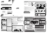
MONITOR

XVM-H6D

CONNECTION BOX

XA-116

REMOTE COMMANDER

RM-X125

SPECIFICATIONS

Monitor

System

Liquid crystal color display

Drive system

TFT-LCD active matrix
system

Picture size

5.8 inches wide screen (16:9)
124 

×

 73 mm, 147 mm

(5 

×

 2 

7/8

 in., 5 

7/8

 in.)

(w/h, d)

Picture segment

280,800 (w 1200 

×

 h 234) dots

Power requirements

12 V DC car battery
(negative ground)

Current drain

Approx. 600 mA

Dimensions

160 

×

 98 

×

 30 mm

(6 

3/8


×

 3 

7/8


×

 1 

1/8

 in.)

(w/h/d)

Operating temperature

5 °C – 45 °C
(41 °F – 113 °F)

Mass

Approx. 300 g (11 oz)

Connection box XA-116

Video Output

Video:

75 

 1Vp-p

Video Input 

×

 2 (Input-A, Input-B)

Video:

75 

 1 Vp-p

Dimensions

92 

×

 29 

×

 62 mm

(3 

5/8


×

 1 

3/16


×

 2 

1/2

 in.)

(w/h/d)

Mass

Approx. 100 g (4 oz)

Card remote commander RM-X125

Power requirements

CR2025 lithium battery

Operable range

Approx. 2.5 m (8.22 ft.)

Dimensions

56 

×

 89 

×

 7 mm

(2 

1/4


×

 3 

5/8


×


9/32

 in.)

(w/h/d)

Mass

Approx. 25 g (1 oz)
(including batteries)

Supplied accessories

Connection box XA-116 (1)
Card remote commander RM-X125
   (with supplied battery) (1)
Power supply cord (1)
Extension cable (5 m) (1)
Mounting plate (1)
Collar (1)
Screws (4)
Operating Instructions (1)

Design and specifications are subject to change
without notice.

Ver 1.0  2002. 07

9-874-136-01

2002G0400-1

© 2002. 07

HEADREST MONITOR

Sony Corporation

e Vehicle Company

Published by Sony Engineering Corporation

Summary of Contents for XVM-H6

Page 1: ...tion box XA 116 Video Output Video 75 Ω 1Vp p Video Input 2 Input A Input B Video 75 Ω 1 Vp p Dimensions 92 29 62 mm 3 5 8 1 3 16 2 1 2 in w h d Mass Approx 100 g 4 oz Card remote commander RM X125 Power requirements CR2025 lithium battery Operable range Approx 2 5 m 8 22 ft Dimensions 56 89 7 mm 2 1 4 3 5 8 9 32 in w h d Mass Approx 25 g 1 oz including batteries Supplied accessories Connection bo...

Page 2: ...Level Adjustment 10 4 DIAGRAMS 4 1 Block Diagram Video Section 11 4 2 Block Diagram Display Section 12 4 3 Printed Wiring Board Display Section 1 2 14 4 4 Printed Wiring Board Display Section 2 2 15 4 5 Schematic Diagram Display Section 1 3 16 4 6 Schematic Diagram Display Section 2 3 17 4 7 Schematic Diagram Display Section 3 3 18 4 8 IC Block Diagrams 19 5 EXPLODED VIEW 5 1 Main Section 23 6 ELE...

Page 3: ... instruction manual 6 Location of Controls 1 POWER button 8 2 INPUT button 8 Press to select the input source 3 MENU button 10 Press to adjust the various display settings 4 F f buttons 8 10 5 Receptor for the card remote commander 6 Monitor connector Monitor ...

Page 4: ... on how to replace the batteries page 15 7 MODE button 9 Press to change the screen mode 8 INPUT button 8 Press to select the input source 9 POWER button 8 Card remote commander RM X125 0 MENU button 10 Press to adjust the various display settings qa F f buttons 8 10 ...

Page 5: ...ection Box XA 116 Front Extension cable 5 m 4 Pin Power connector Fuse 0 1 A Fuse 3 A Yellow 5 m Blue 1 m Red 5 m To a metal surface of the car chassis To car battery 12 V To ignition switch ACC position Media Center FM AM Receiver XAV 7W optional A Power supply cord To Video input To Video output To Audio input L R 1 Video signals of DVX 100 are output to XVM H6 and audio signals are output to XA...

Page 6: ...o the following sequence Note Follow the disassembly procedure in the numerical order given 2 1 BOTTOM CABINET 2 1 BOTTOM CABINET Page 6 SET 2 2 DISPLAY BOARD Page 7 2 3 LIQUID CRYSTAL DISPLAY PANEL LCD1 Page 7 1 screw P 2x5 2 screw tapping P 2x6 5 bottom cabinet 3 claw 4 claw ...

Page 7: ...7 XVM H6 2 2 DISPLAY BOARD 2 3 LIQUID CRYSTAL DISPLAY PANEL LCD1 4 screw B 2x3 5 DISPLAY board 3 Removal the solder 2 U6 1 M1 1 screw I 2x3 2 bracket 4 insulation plate B 3 LCD1 ...

Page 8: ...n 2 Connect digital voltmeter to the C320 position of L305 3 Adjust VR 5 so that the reading on the voltmeter stands at the specified value Specified value 5 00 0 05 V 3 4 FREQUENCY ADJUSTMENT This frequency adjustment on the DC DC converter is only performed if there is switching noise mixed on the screen Adjust the semi fixed resistor VFRQ to a position in which no noise appears on the screen 3 ...

Page 9: ...hat the reading on the voltmeter is at 1 40 0 04 V 3 13 RGB GAIN 1 ADJUSTMENT 1 Display gray scale on the monitor screen 2 Connect digital voltmeter to pin 28 of IC U600 3 Adjust VRGB so that the reading on the voltmeter is at 2 05 0 04 V 3 14 RGB GAIN 2 ADJUSTMENT 1 Display 5 step gray scale on the monitor screen 2 Connect oscilloscope to pin 21 of IC U600 3 Adjust the semi fixed resistorVRGB so ...

Page 10: ... 4 40 0 04 V B 1 43 0 04 V 3 18 BLANK LEVEL ADJUSTMENT 1 Display gray scale on the monitor screen Set the screen to the Normal mode Adjustment Location VFRQ VR 5 DISPLAY BOARD CONDUCTOR SIDE L305 C302 VSUR VCOA VCOL VTIN VCOM VSUB VCNT VPIC VBRI VRGB VGA1 VFREQ VCDC VGA2 VHIG Q703 Q701 COMPONENT SIDE U2 U600 VLOW If not black on the right and left ends adjust VHIG and VLOW so that black vertical b...

Page 11: ...VPIC SHARPNESS VCNT CONTRAST VRGB RGB GAIN VSUB B LEVEL VSUR R LEVEL VGA1 γ 0 VGA2 γ 2 γ AMP VDD 3 3V Q501 Q502 Q503 RC3 SCK SCL RC6 TX CK RC4 SD1 SDA RB4 UC CS UC WR UC SIN UC SCK RB3 RB2 RB1 SYSTEM CONTROL U501 1 2 SCLK CS SIN RST CS WR SIN SCLK XIN XOUT 8 9 Y3 4MHz TO OTHER CHANNELS CONTROL DATA BUS EVR DATA DECODER U506 PWM1 EXD XD VSYNC HSYNC PWM2 PWM3 PWM4 L501 BLKA VC0 VC1 VC2 SW ACC_OUT BR...

Page 12: ...POL NPC C SYNC H SYNC V SYNC COM_OUT X V Z A B C B G R SELECTOR U602 VLOW BLACK LEVEL LOW VCOA COM LEVEL VFRQ DC DC FREQUENCY VCDC COM BIAS VFREQ PLL FREERUN VR 5 5V PLL CLOCK VHIG BLACK LEVEL HIGH VCO U704 D702 BLK POL 2 SYNC HOO_IN VOUT VIN VDFOUT VOFIN PD VD VH VCOM VCOO PN L702 Q604 HDOUT1 VSYNC SIDE1 JUST ZOOM SIDED1 JUST ZOOM RESET STB CHP1 DEH DVE1 DVE2 DEV3 CPV STV1 STV2 RED2 RED1 GREEN2 G...

Page 13: ...tolerances Waveforms are taken with a oscilloscope Voltage variations may be noted due to normal produc tion tolerances Circled numbers refer to waveforms Signal path g VIDEO for printed wiring boards X parts extracted from the component side Y parts extracted from the conductor side Pattern from the side which enables seeing Note The components identified by mark 0 or dotted line with mark 0 are ...

Page 14: ...743 D301 D408 D407 D409 FB602 D303 Q503 B C E Q701 E C B U702 B C E Q502 B C E Q514 B C E Q511 K5 POWER K4 MODE K3 MENU K1 K2 E C B Q770 E C B Q504 E C B B C E C703 C705 C710 R707 R706 R631 C625 C624 R635 C627 R662 R651 R654 C635 R648 R5 R612 R667 C620 R625 C610 C609 R661 R609 C666 R610 R640 C628 C418 C503 C502 C516 C517 R460 R459 R455 R451 R448 C319 Q301 E C B Q211 W110 C306 R301 R201 C301 R303 C...

Page 15: ...711 C721 C729 C723 R722 R731 R729 R728 R737 R738 R739 R740 C728 R623 R626 R772 R715 R754 R458 R669 R510 R540 R536 R535 R561 R543 R509 R8 R508 R551 R501 R502 R402 R11 R9 R401 R28 D410 D501 R760 C313 L302 C302 R309 L304 B C E Q408 L401 C16 C5 C453 C641 C640 C701 C748 C605 C318 C309 C320 C311 C315 C200 C704 C307 C312 C317 B E Q3 Q2 Q410 E C B Q411 B C E Q604 1 1 5 10 15 J18 10 J1 D3 B C E Q409 B C E ...

Page 16: ...R440 R439 R438 R437 C525 R316 C516 R16 Y4 C511 C510 C513 C522 D408 D409 R509 R561 R531 R8 R508 R1 R535 R536 R540 C1 C2 C523 R512 2 2k 220 16V C507 W100 W101 W102 W107 W108 W109 W111 D407 J2 L401 R28 R11 R402 R552 R441 R18 R442 R539 R563 R543 Q211 R17 Q504 D501 C13 R470 Q409 Q3 M1 U501 R558 Q514 D3 J1 J18 M2 U504 15k 15k Note The components identified by mark 0 or dotted line with mark 0 are critic...

Page 17: ...616 R623 R624 C617 R626 R627 C618 C619 C622 R633 R634 C623 R643 R644 R640 R641 C628 C632 C634 R630 R631 R628 R629 L602 Q501 Q502 Q503 R520 R510 R511 R513 L501 U503 C509 C508 R507 R502 R501 R503 R504 R505 R506 Y3 C503 C502 R447 R446 R445 R449 R451 D412 R453 R455 R456 D413 R459 R517 R448 VCOM VRGB VPIC VGA1 VGA2 VSUB VSUR VCOL VTIN VBR1 VCNT C668 C663 C626 R636 C517 D410 R452 D411 R450 R458 R460 R62...

Page 18: ... RL U704 C729 C725 R772 C761 C770 VCDC Q701 C702 LCD1 U701 W104 W105 W106 U3 Q703 C301 C302 R302 R314 R313 C304 C305 R308 R307 C205 C202 R214 R215 R202 R203 R216 C201 R201 C200 C521 L301 C306 C307 R310 R309 D301 D302 D303 D304 C309 C311 C312 R760 C310 L302 C313 C315 L304 C317 C318 L305 C319 C320 F201 R553 Q510 L200 Q511 R556 R12 R13 R554 R22 W110 D702 W719 L712 R765 D1 C760 C706 C720 L706 C742 L70...

Page 19: ...SS VCC WP SCL SDA I O CONTROL LOGIC 12 11 10 8 9 14 13 1 2 3 6 7 4 5 CS WR R SIN SCLK OC GND PWM3 PWM2 PWM1 PWM4 VCC XIN XOUT INPUT REGISTER CONTROL CIRCUIT PWM REGISTER 8 BIT PWM CIRCUIT 4 BIT RATE MULTIPLIER 12 BIT PWM CIRCUIT OSCILLATION CIRCUIT LOWER BYTE REGISTER UPPER BYTE REGISTER 1 2 DIVIDER TO OTHER CHANNELS 2 6 5 8 7 3 4 OUT IN C OUT IN C 1 LOGIC LEVEL CONVERTER COMMON INH VEE VSS VDD CH...

Page 20: ...RAM WRITING CONTROL ADDRESS CHANGEOVER SWITCH VRAM CG ROM CHARACTER OUTPUT 12 13 14 15 16 11 17 18 19 20 BLKC TESTO BLKB VC3 BLKA VC2 VC1 VC0 VSYNC HSYNC SCLK CS SIN RESET VDD SDR XD EXD TEST GND 1 2 DECODER LOGIC LEVEL CONVERSION 3 4 5 7 8 6 DECODER LOGIC LEVEL CONVERSION DECODER LOGIC LEVEL CONVERSION 14 13 12 11 10 9 15 16 VCC 2Y1 2Y0 3Y1 3Z 3Y0 E VEE GND 2Z 1Z 1Y1 1Y0 S2 S3 S1 ...

Page 21: ...OMP COMP MATRIX INT EXT SW γ AMP γ AMP INV INV VREF DEMOD R Y G Y B Y SYNC IN Y C Y C BGP F F Y R Y G Y B Y PAL ON P N N P CHROMA OUT ACC FILTER B Y R Y KILLER FILTER BURST OUT COLOR C IN IDENT FILTER VIDEO IN CONTRAST TRAP PICTURE AGC OUT AGC FILTER CLAMP F ADJ VCC1 G IN R IN B IN SW COMMON OUT COMMON AMPLITUDE ADJUST SYNC SEP SYNC OUT SYNC IN FRP SUB BRIGHT R SUB BRIGHT B BRIGHT GAMMA 0 GAMMA 2 ...

Page 22: ...DOUT VDFIN HSYNC HDOUT1 HDSEL VSYNC INT EXT VOLUME BLK POL1 POL2 ZOOM VDFOUT DVDD CPV OEV3 OEH STH OEV1 OEV2 STV BP DVSS PD VCOM VC00 DVDD AVDD DPOV1 DPOV2 DVDD AVSS AGS ZOOM SEL JUST SIDE1 UONS SIDE2 VPOS3 VPOS2 PLL CPH2 CPH3 CPH1 SYNC DVDD PN RESET PAIR DMODE COPY HDCT DVSS HPOS4 VPOS0 HPOS3 HPOS2 HPOS1 HPOS0 VPOS1 PLL CLOCK VCC PLLCLK PHASE COMPARATOR CLOCK SELECT CIRCUIT CLOCK DIVIDER HORIZONT...

Page 23: ...UT M3X6 5 7 627 553 38 SCREW B2X3 BN NOTE The mechanical parts with no reference number in the exploded views are not supplied Items marked are not stocked since they are seldom required for routine service Some delay should be anticipated when ordering these items XX and X mean standardized parts so they may have some difference from the original one Color Indication of Appearance Parts Example K...

Page 24: ... 1 135 960 11 CERAMIC CHIP 10uF 10 25V C424 1 162 964 21 CERAMIC CHIP 0 001uF 5 50V C425 1 135 960 11 CERAMIC CHIP 10uF 10 25V C453 1 128 992 11 ELECT 47uF 20 25V C501 1 127 820 11 CERAMIC CHIP 4 7uF 16V C502 1 162 920 11 CERAMIC CHIP 27PF 5 50V C503 1 162 920 11 CERAMIC CHIP 27PF 5 50V C504 1 165 908 11 CERAMIC CHIP 1uF 10 10V C505 1 107 826 11 CERAMIC CHIP 0 1uF 10 16V C506 1 135 960 11 CERAMIC ...

Page 25: ... CERAMIC CHIP 0 001uF 5 50V C722 1 107 826 11 CERAMIC CHIP 0 1uF 10 16V C723 1 164 739 11 CERAMIC CHIP 560PF 5 50V C725 1 162 965 21 CERAMIC CHIP 0 0015uF 5 50V C726 1 107 826 11 CERAMIC CHIP 0 1uF 10 16V C727 1 162 924 11 CERAMIC CHIP 56PF 5 50V C728 1 107 826 11 CERAMIC CHIP 0 1uF 10 16V C729 1 107 826 11 CERAMIC CHIP 0 1uF 10 16V C742 1 165 908 11 CERAMIC CHIP 1uF 10 10V C743 1 107 826 11 CERAM...

Page 26: ...8 727 11 METAL CHIP 30K 5 1 10W R11 1 216 835 11 METAL CHIP 15K 5 1 10W R12 1 216 865 11 METAL CHIP 3K 5 1 10W R13 1 216 865 11 METAL CHIP 3K 5 1 10W R14 1 218 271 11 METAL CHIP 2K 5 1 10W R15 1 216 821 11 METAL CHIP 1K 5 1 10W R16 1 216 809 11 METAL CHIP 100 5 1 10W R17 1 216 812 11 METAL CHIP 180 5 1 10W R18 1 216 845 11 METAL CHIP 100K 5 1 10W R21 1 216 841 11 METAL CHIP 47K 5 1 10W R22 1 216 8...

Page 27: ...1K 5 1 10W R624 1 216 821 11 METAL CHIP 1K 5 1 10W R625 1 216 855 11 METAL CHIP 680K 5 1 10W R626 1 216 821 11 METAL CHIP 1K 5 1 10W R627 1 216 821 11 METAL CHIP 1K 5 1 10W R628 1 216 842 11 METAL CHIP 56K 5 1 10W R629 1 216 840 11 METAL CHIP 39K 5 1 10W R630 1 216 842 11 METAL CHIP 56K 5 1 10W R631 1 216 840 11 METAL CHIP 39K 5 1 10W R632 1 242 957 11 METAL CHIP 5 6M 5 1 10W R633 1 216 833 11 MET...

Page 28: ...74HC4053D U602 9 885 026 44 IC DG419DY U610 9 885 026 39 IC AME8805AEFT U701 9 885 025 64 IC LF353MX U702 9 885 025 65 IC MN13821 U704 8 759 575 16 IC LMC7101BIM5X CERMET RESISTOR VBR1 1 227 231 11 RES ADJ CERMET 50K VCDC 1 227 231 11 RES ADJ CERMET 50K VCNT 1 227 231 11 RES ADJ CERMET 50K VCOA 1 227 231 11 RES ADJ CERMET 50K VCOL 1 227 231 11 RES ADJ CERMET 50K VCOM 1 227 231 11 RES ADJ CERMET 50...

Page 29: ... CORD CONNECTION POWER including F901 F902 3 242 086 11 MANUAL INSTRUCTION ENGLISH FRENCH SPANISH 3 245 767 01 BRACKET MAIN 3 245 768 01 FRAME ORNAMENT 9 885 026 85 LID BATTERY CASE for RM X125 0F901 1 532 419 11 FUSE 3A 250V 0F902 1 532 404 11 FUSE 0 1A 250V The components identified by mark 0 or dotted line with mark 0 are critical for safety Replace only with part number specified ...

Page 30: ... HISTORY Clicking the version allows you to jump to the revised page Also clicking the version at the upper on the revised page allows you to jump to the next revised page Ver Date Description of Revision 1 0 2002 07 New ...

Reviews: