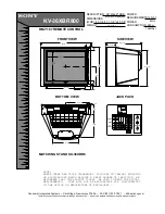
background image

- 1 -

SERVICE MANUAL

FE-2


CHASSIS

MODEL

COMMANDER

DEST

CHASSIS NO.

KV-29LS40B

RM-947

FR

SCC-Q54V-A

KV-29LS40E

RM-947

ESP

SCC-Q53W-A

MODEL

COMMANDER

DEST

CHASSIS NO.

KV-29LS40K

RM-947

OIRT

SCC-Q51S-A

RM-947

KV-29LS40

Summary of Contents for Trinitron KV-29LS40K

Page 1: ...SERVICEMANUAL FE 2CHASSIS MODEL COMMANDER DEST CHASSIS NO KV 29LS40B RM 947 FR SCC Q54V A KV 29LS40E RM 947 ESP SCC Q53W A MODEL COMMANDER DEST CHASSIS NO KV 29LS40K RM 947 OIRT SCC Q51S A RM 947 KV 29LS40 ...

Page 2: ...D THE ANODE CAP TO THE METAL CHASSIS CRT SHIELD OR THE CARBON PAINTED ON THE CRT AFTER REMOVAL OF THE ANODE CAP WARNING AN ISOLATION TRANSFORMER SHOULD BE USED DURING ANY SERVICE WORK TO AVOID POSSIBLE SHOCK HAZARD DUE TO LIVE CHASSIS THE CHASSIS OF THIS RECEIVER IS DIRECTLY CONNECTED TO THE POWER LINE SAFETY RELATED COMPONENT WARNING COMPONENTS IDENTIFIED BY SHADING AND MARKED ON THE SCHEMATIC DI...

Page 3: ...r p p A n o i t c e l f e d e e r g e d 4 0 1 t u p t u o d n u o S r e k a e p s t f e L d n a t h g i R S M R W 7 x 2 r e w o P c i s u M W 4 1 x 2 R A E R s l a n i m r e T t u p t u O t u p n I s n o i t a c i f i c e p S l a r e n e G r o t c e n n o c o r u E n i p 1 2 1 d r a d n a t s C E L E N E C s l a n g i s o e d i V d n a o i d u A r o f s t u p n I B G R r o f s t u p n I o i d u A ...

Page 4: ...2 Open 13 Ground red 14 Ground blanking 15 _ _ Red input 0 7 3dB 75 ohms positive _ S signal Chroma input 0 3 3dB 75 ohms positive 16 Blanking input Ys signal High state 1 3V Low state 0 0 4V Input impedence 75 ohms 17 Ground video output 18 Ground video input 19 Video output 1V 3dB 75ohms positive sync 0 3V 3 10dB 20 _ _ Video input 1V 3dB 75ohms positive sync 0 3V 3 10dB _ Video input Y S signal...

Page 5: ... E 7 0 E 8 0 E 9 0 E 0 1 E 1 1 E E M I T G N I K R O W S R U O H S E T U N I M P C O A N P V O C N Y S V R K I C I I M V N E L G N U J R E N U T P D N U O S V 8 5 5 2 0 5 5 2 0 5 5 2 0 5 5 2 0 5 5 2 0 5 5 2 0 5 5 2 0 5 5 2 0 5 5 2 0 5 5 2 0 0 0 0 0 0 0 0 0 0 0 2 1 1 e g a s s e M r o r r E D E L e d o C r o r r e o N 0 0 d e v r e s e R 1 0 n o i t c e t o r P t n e r r u C r e v O P C O 2 0 d e s...

Page 6: ...just now then press OK and correct any slant of the picture between 5 and 5 by pressing or Finally press OK to store 8 First Time Operation 5 The Auto Tuning menu appears on the screen Press the OK button to select Yes 6 The TV starts to automatically search and store all available broadcast channels for you This procedure could take some minutes Please be patient and do not press any buttons othe...

Page 7: ...epeatedly v V B or b to adjust it and finally press OK to store the new adjustments This menu also contains two submenus as following Mode b v Personal for individual settings Rock Pop Jazz Detail Adjustment b v Dolby Virtual v Off Normal v On Simulates the sound effect of Dolby Pro Logic surround v Auto volume v Off Volume level changes according to the broadcast signal v On Volume level of the c...

Page 8: ...ress b and then proceed in the same way as in step 7b of the section Switching On the TV and Automatically Tuning PROGRAMME LABELS The Programme Labels option in the Set Up menu allows you to name a channel using up to five characters letters or numbers To do this 1 After selecting the option press b then press v or V to select the programme number with the channel that you wish to name 2 Press b ...

Page 9: ... 101 98 TELETEXT Index Programme News Sport Weather 25 153 101 98 TELETEXT Index Programme News Sport Weather 25 153 101 98 TELETEXT Index Programme News Sport Weather 25 153 101 98 17 Connecting Optional Equipment Using the following instructions you can connect a wide range of optional equipment to your TV set Connecting cables are not supplied Additional Information 1 2 S VHS Hi8 DVC Camcorder ...

Page 10: ... page 2 Switch on the connected equipment 3 To watch the picture of the connected equipment press the button repeatedly until the correct input symbol appears on the screen Symbol Input Signals 1 Audio video input signal through the Scart connector D RGB input signal through the Scart connector D This symbol appears only if an RGB source has been connected 2 Audio video input signal through the Sc...

Page 11: ...nd select Reset to return to the factory settings No picture or no menu information from equipment connected to the Scart connector Check that the optional equipment is on and press the button repeatedly on the remote control until the correct input symbol is displayed on the screen Good picture no sound Press the button on the remote control Check that TV Speakers is On on the Sound Adjustment me...

Page 12: ... Removal and Refitting To remove lift the main bracket rear slightly and slide the chassis away from the beznet Ensure that the interconnecting leads are released from their purse locks to prevent damage being caused When refitting the chassis ensure that the main bracket is located in the beznet guide slots before sliding the chassis forwards Refit the interconnecting leads in their respective pu...

Page 13: ...ut servicing Remove the two screws fixing the user control module to the side of the set The control module can then be removed by sliding it towards the rear of the set allowing access to the H2 Board Screws Remove the screw securing the PWB to the main bracket Clip 2 4 A Board PWB Removal Step 2 2 3 A Board PWB Removal Step 1 2 6 Side Control Module Removal 2 5 Service Position ...

Page 14: ...e Anode Cap 2 7 Picture Tube Removal WARNING BEFORE REMOVING THE ANODE CAP High voltage remains in the CRT even after the power is disconnected To avoid electric shock discharge CRT before attempting to remove the anode cap Short between anode and CRT coated earth ground strap Coated Earth Ground Strap 1 Discharge the anode of the CRT and remove the anode cap 2 Release the EHT lead from its CRT su...

Page 15: ...o Green and verify the condition 6 When the position of the deflection yoke has been determined fasten the deflection yoke with the screws 7 If the beam does not land correctly in all the corners use a magnet to correct it See Fig 3 4 When complete readjustment is necessary or a new picture tube is installed carry out the following adjustments Unless there are specific instructions to the contrary...

Page 16: ...e each other The movement of the magnets interact with each other and so the respective dot position should be monitored while carrying out this adjustment Use the H STAT VR to adjust the Red Green and Blue dots so that they coincide at the centre of the screen by moving the dots in the horizontal direction G B R G B R G B R G B R G B R G B R 3 2 Convergence Operation of the BMC Hexapole magnet Pr...

Page 17: ...ertical static convergence 1 Remove the deflection yoke spacer 2 Tilt the deflection yoke as indicated in the figure below and optimise the geometry Tilting the DY Up and Down will balance the upper and lower pin adjustment Tilting the DY Left and Right will balance the H Trap adjustment 3 Re install the deflection yoke spacer Screen Corner Convergence TLH pieces Deflection Yoke a b d Permalloy As...

Page 18: ...yback Transformer to the point where the OSD menu indication shows OK Layout of each control 1 Input an all white signal from the pattern generator 2 Enter into the Service Mode by pressing TEST TEST and MENU on the Service Commander 3 Select Service from the on screen menu display and press the right arrow button on the remote commander 4 The Service menu will appear on the screen See Page 19 5 S...

Page 19: ...A F I t s u j d A C G A e t u m o t u A n i a G o i d u A g n i t a G L 5 1 6 1 0 1 0 0 E C I V R E S R t e s f f O G t e s f f O e v i r D R e v i r D G e v i r D B q e r F k a e P y a l e D a m u L 0 C S k a e P e t i h W t n o c b u S t h g i r b u S l o c b u S p r a h s b u S r B f f o t u C D S O r B T X T r B 3 6 0 3 6 0 3 6 0 3 6 0 3 6 0 3 0 5 1 0 3 0 5 1 0 5 1 0 3 6 0 3 6 0 3 6 0 3 6 0 5 ...

Page 20: ...oltage is 3 5volts 0 3volts 4 If adjustment is required then re adjust theAGC variable resistor located at the top rear of the FRONTEND to obtain a voltage of 3 5V 0 3V 1 Enter into the Geometry service menu 2 Select and adjust each item in order to obtain the optimum image Print side of A board Deflection System Adjustment V SIZE V LIN S CORRECTION V CENTRE H CENTRE H SIZE PIN AMP PIN PHASE CORNE...

Page 21: ...d a s s e n t h g i r B b u S 4 1 t n e m t s u j d a n o i t i s o P H t x e T 5 1 t s e T l i o C n o i t a t o R 6 1 0 5 l e v e l e r u t c i P 9 1 e l b a s i D e l b a n E e d o M y r o t c a F 1 2 R K E D A n o i t a n i t s e D 2 2 L B n o i t a n i t s e D 3 2 R K E D A n o i t a n i t s e D 4 2 U n o i t a n i t s e D 5 2 R K E D A n o i t a n i t s e D 6 2 L B n o i t a n i t s e D 7 2 ...

Page 22: ... AGC SCL SDA VIDEO IC004 SDA 6 SCL 5 7 WP 71 SCL 72 SDA 28 CVBS2 CVBSY2 3 AGC 53 B2 UIN 1 MODE1 80 MODE2 52 G2 YIN 51 R2 VIN 38 C4 50 INSSW2 32 CVBS1 37 CVBS4Y4 45 AUDIO 1 34 CVBS3 8 11 7 29 15 16 40 36 20 2 BLUE MODE MODE GREEN RED C2 IN BLK V IN 1 Y V IN 2 TU101 R IN 1 STBY 70 2 FB D513 15V RECT D638 5 SDA CS SCL AGC IC201 MSP3410D PP B4 SC1 OUT R 37 SC1 OUT L 36 63 XTAL OUT 62 XTAL IN 47 SC3 IN...

Page 23: ...IGH RIPPLE Les composants identifiés par une trame et par une marque sont d une importance critique pour la sécurité Ne les remplacer que par des pièces de numéro spécifié specified Note The components identified by shading and marked are critical for safety Replace only with the part numbers specified in the parts list Note CVM Board A Board S1 Board VM C H D1 A J A2 N D A1 D2 C A 5 1 BLOCK DIAGR...

Page 24: ...00p C633 XX R658 1W RN 10M R613 FBIU4D7M1 B 4 D625 1 10W 10 R624 1 10W 10 R654 1 10W 10k R622 1 10W 10k R629 1 1uH FB601 1 1uH FB604 1 1uH FB605 1 2 3 CN642 XX THP601 RK14V1 D618 RK14V1 D619 FMW 2109LF654 D638 G2SBA60L 5700 D614 250V 1000p C603 250V 1000p C604 JW632 12 5MM JW606 12 5MM P6KE200ASY D628 XX C602 1 2 CN607 AC out AC out JW630 XX JW631 XX XX JW604 XX JW605 1 2 3 4 T601 XX R602 0uH FB60...

Page 25: ... R551 2W 1k R591 47k R555 1 10W 3 3k R500 1 10W 15k R524 1 10W 12k R527 1 10W 22k R533 1 10W 100k R522 1 10W 680k R523 XX JR505 1 4W FPRD 0 47 R595 1 4W FPRD 3 3 R548 22uH L502 270uH L505 R547 7 5 1 2 3 4 5 WHT 5P CN508 BY228RAS20 10 D536 EL1Z D534 EGP20G D501 EGP20G D513 EGP20G D514 ST2310DHI Q533 50V 1000p C519 50V 1000p B C583 R520 47 2W 1 10W CHIP 10k R502 1 10W 10k R529 1 10W 33k R530 1 10W 4...

Page 26: ...4700p C436 25V 0 47 C235 50V 47p C221 25V 0 33 C230 XX R253 XX R254 1 10W 47 R220 1 10W 120 R416 470 R450 1 10W 470 R451 1 10W 470 R1230 1 10W 470 R1232 L410 100 1 10W CHIP 0 R406 C215 1 5p 50V C217 1 5p 50V 1 10W 6 8k R212 1 10W 6 8k R233 1 10W 6 8k R234 1 10W 6 8k R251 1 10W 6 8k R252 1 10W 10k R217 1 10W 10k R420 1 10W 10k R428 1 10W 10k R430 1 10W 10k R431 1 10W 10k R433 1 10W 10k R434 1 10W 1...

Page 27: ...V 1000 C1228 50V 220p B C1229 50V 220p B C1230 XX C1231 50V 1000p C428 25V 0 01 C026 50V 0 022 F C1209 50V 0 022 F C1211 XX C524 R072 0 22 C449 100 1 10W R073 XX XX R558 1 10W 3 3k R032 1 10W 3 3k R103 1 10W 4 7k R557 1 10W 6 8k R014 1 10W 10k R092 1 10W 10k R096 1 10W 10k R1202 1 10W 15k R1207 1 10W 15k R1210 1 10W 22k R056 XX R091 1 10W 27k R036 1 10W 470k R448 1 10W 1M R012 0 JR4 0 JR7 XX JR9 C...

Page 28: ...M 8 3 5 D 6 E 2 1 6 D 5 G 5 2 6 D 6 H R O T S I S N A R T 2 3 5 Q 4 D 9 0 6 Q 6 J 4 0 0 C I 2 H 1 0 0 D 2 I 6 1 0 D 2 J 4 0 1 D 2 E 9 3 2 D 3 D 2 1 4 D 3 D 7 2 4 D 4 A 6 0 5 D 4 D 9 3 5 D 5 B 3 1 6 D 6 J 7 2 6 D 7 K 3 1 0 Q 3 I 3 3 5 Q 6 A 0 1 2 1 Q 3 H 1 0 4 C I 3 I 2 0 0 D 3 I 8 1 0 D 3 I 5 0 1 D 1 A 2 0 4 D 3 E 3 1 4 D 3 C 8 2 4 D 3 C 7 0 5 D 2 M 1 4 5 D 5 F 4 1 6 D 8 K 8 2 6 D 7 L 4 1 0 Q 1 L ...

Page 29: ... D710 D709 RD6 8ESB2 D708 50V 0 01 C703 50V 10 C702 1 4W 10k R702 250V PT 0 1 C701 D706 1SS83TA D707 1SS83TA D702 1SS83TA 500V 0 001 B C705 250V 10 C710 1 4W 1M R701 10k R1805 CHIP 0 022 C1803 50V 8 7 6 5 4 3 2 1 M5216P IC1801 100 R1801 1 10W 10k R1809 10k R1808 XX R1802 10k R1807 CHIP 50V 10 C1804 50V 47p CH C1805 1 2 3 WHT 3P CN1801 ROT NC ROT 10k R1810 1 2 3 4 5 6 7 WHT 7P CN703 NS CORRECT 1K G...

Page 30: ...C D E F G H I J K L M N 1 2 3 4 5 6 7 8 9 10 11 30 C Printed Wiring Board Conductor Side F2 Printed Wiring Board Conductor Side H2 Printed Wiring Board Conductor Side VM Printed Wiring Board Conductor Side ...

Page 31: ...02 CHIP 1k R1913 50V 10 C1903 PT 2200p C1904 0 047 C1905 1SS133 D1903 CHIP 1M R1912 CHIP 10k R1911 1SS133 D1904 CHIP 0 R1910 RD15ESB2 D1905 2SC3840K Q1903 D1906 ER106T B D1907 UF106GT B D1908 630V PT 0 022 C1915 CHIP 100k R1923 CHIP 100k R1924 CHIP 100k R1925 L1901 C1914 C1913 3W 6 8k R1918 R1921 500V 470p B C1917 C1912 0 47 C1911 2W RS 6 8K R1967 2W RS 5 6K R1969 1 4W 680k R1909 1 2 3 4 6 T1901 X...

Page 32: ...6 2SC2412K QR 2SC2412K T 146 QR 2SC2412K T 146 R SE 135N SE135N LF4 TDA9394H TOP209P BF421 AMMO 2SA1091 O 2SC2785 HFE 2SA933AS QRT 2SAG33ASQT 2SA933AS RT 2SC1740S RT IRF614 005 IRF614 037 IRF620 8 7 6 5 1 3 4 TOP VIEW 2 1 2 3 1 V OUT 2 V IN 3 GND TOP VIEW E C B C B E B C E B C E LETTER SIDE B C E MARKING SIDE VIEW 64 41 1 24 80 65 25 40 MSP3410G PP B8 MSP3411G PP B9 7 1 1 32 33 64 STV9379 2SK2251 ...

Page 33: ...2 RD9 1ES B3 RD10ESB2 RD15ES T1B2 1SS119 25TD 1SS133T 77 1SS355TE 17 RD12SB2 UDZS TE 17 4 7B UDZS TE 17 5 6B UDZS TE 17 6 8B UDZS TE 17 9 1B UDZ TE 17 22B UF4005PKG23 CATHODE ANODE CATHODE ANODE CATHODE ANODE CATHODE ANODE DAN202K DAN202K T146 MA8330 TX D4SB60L F AK04 V1 AU 01Z V1 BYD33G BYD33G AMMO DINL20 TA DINL20 U TA2 DINL40 U TR2 ERB44 06TP1 EGP20G EG 1Z V1 EL1Z ERD28 06S ERD28 06S ERC06 15SL...

Page 34: ...F Latch Centre Osc SS F B Timer TSD OCP Control Logic Level Shift Sel 34v ref 5v 15v 8v Driver Reg 10v 18 8 14 16 15 10 12 11 9 A BOARD IC401 IC531 LM393DT A BOARD IC601 MCZ3001D A BOARD IC1201 TDA7495S 9 8 11 5 Pwr Gnd MUTE STBY PROTECTION 14 7 Sgn Gnd 1 10 60K 12 15 13 Pwr Gnd Vss ...

Page 35: ... 35 1 1 571 433 21 SWITCH PUSH AC POWER 2 4 202 531 01 AC CORD LOCK SC 3 1 765 286 11 CORD POWER 4 4 206 048 02 BRACKET MAIN 5 1 424 733 11 COIL PFC CHOKE 65MMH 6 1 453 308 51 TRANSFORMER ASSY FLYBACK NX 4521 Z2B4 7 8 598 535 20 FRONTEND BTF EF411 KV 29LS40B 8 598 533 10 FRONTEND BTF EC411 KV 29LS40E K 8 A 1052 332 A A BOARD COMPLETE KV 29LS40B A 1052 327 A A BOARD COMPLETE KV 29LS40E K 9 A 1624 1...

Page 36: ...A ROTATION RT 200 63 A 1645 045 A VM BOARD COMPLETE 64 A 1639 019 A C BOARD COMPLETE 65 4 369 318 21 SPRING TENSION 66 1 416 654 21 COIL DEMAGNETIC 67 4 203 390 11 CUSHION DGC 68 4 204 768 02 HOLDER DGC 29 69 8 453 011 11 NECK ASSY NA299 M 70 4 203 022 01 HOLDER HV 71 1 251 537 22 CAP ASSY HIGH VOLTAGE 72 3 704 495 03 SPACER DY 73 4 046 765 12 SCREW TAPPING 7 CROWN WASHER 74 4 308 870 00 CLIP LEAD...

Page 37: ... this model and therefore do not appear in the Parts List 37 A BOARD COMMON Parts List Parts common to all models listed in this manual 38 A BOARD VARIANT Parts List PParts that belong only to the model specified Model KV 29LS40B 45 KV 29LS40E 45 KV 29LS40K 45 F2 BOARD COMPLETE Parts List 45 C BOARD COMPLETE Parts List 45 VM BOARD COMPLETE Parts List 46 H2 BOARD COMPLETE Parts List 47 MISCELLANEOU...

Page 38: ... SHORT CHIP 0 C214 1 163 253 11 CERAMIC CHIP 120PF 5 00 50V C215 1 163 084 00 CERAMIC CHIP 1 5PF 0 25PF 50V C216 1 163 117 00 CERAMIC CHIP 100PF 5 00 50V C217 1 163 084 00 CERAMIC CHIP 1 5PF 0 25PF 50V C218 1 216 295 91 SHORT CHIP 0 C221 1 163 109 00 CERAMIC CHIP 47PF 5 00 50V C222 1 163 117 00 CERAMIC CHIP 100PF 5 00 50V C223 1 126 965 91 ELECT 22UF 20 00 50V C224 1 163 117 00 CERAMIC CHIP 100PF ...

Page 39: ...0 00 250V C604 1 119 899 51 CERAMIC 1000PF 10 00 250V C605 1 115 785 11 ELECT 470UF 20 00 25V C606 1 117 751 11 ELECT BLOCK 220UF 20 00 450V C607 1 126 964 11 ELECT 10UF 20 00 50V C608 1 126 963 11 ELECT 4 7UF 20 00 50V C610 1 126 941 11 ELECT 470UF 20 00 25V C611 1 163 009 91 CERAMIC CHIP 0 001UF 10 00 50V C612 1 104 571 91 CERAMIC 0 0015UF 10 00 2KV C613 1 104 571 91 CERAMIC 0 0015UF 10 00 2KV C...

Page 40: ...719 069 55 DIODE UDZSTE 175 6B D404 8 719 109 89 DIODE RD5 6ESB2 D420 8 719 069 55 DIODE UDZSTE 175 6B D424 6 500 028 01 DIODE MM3Z9V1ST1 D501 8 719 979 85 DIODE EGP20G D502 8 719 081 90 DIODE PDZ22B 115 D1 A D503 8 719 069 55 DIODE UDZSTE 175 6B D504 8 719 074 43 DIODE BAS316 115 D505 8 719 081 97 DIODE MMDL914T1 D506 6 500 106 01 DIODE PG4003T B D507 8 719 070 59 DIODE PDZ6 8B 115 D512 8 719 302...

Page 41: ...607 6 550 591 01 TRANSISTOR 2SK2543 LBS2SONY Q608 8 729 120 28 TRANSISTOR 2SC1623 L5L6 Q609 8 729 026 49 TRANSISTOR 2SA1037AK T146 R Q1230 8 729 027 56 TRANSISTOR DTC143TKA T146 Q1231 8 729 027 56 TRANSISTOR DTC143TKA T146 Q1232 8 729 026 49 TRANSISTOR 2SA1037AK T146 R Q1233 8 729 026 49 TRANSISTOR 2SA1037AK T146 R F4 A FB603 1 412 911 11 FERRITE 0UH FB604 1 469 578 11 FERRITE 1 1UH FB605 1 469 57...

Page 42: ... 1 216 065 91 RES CHIP 4 7K 5 1 10W R040 1 216 033 00 RES CHIP 220 5 1 10W R041 1 216 025 11 RES CHIP 100 5 1 10W R042 1 216 025 11 RES CHIP 100 5 1 10W R044 1 216 073 91 RES CHIP 10K 5 1 10W R045 1 216 025 11 RES CHIP 100 5 1 10W R046 1 216 025 11 RES CHIP 100 5 1 10W R047 1 216 025 11 RES CHIP 100 5 1 10W R048 1 216 073 91 RES CHIP 10K 5 1 10W R049 1 216 049 11 RES CHIP 1K 5 1 10W R050 1 216 025...

Page 43: ...892 81 METAL OXIDE 1K 5 2W R540 1 212 970 00 FUSIBLE 33 5 1 2W R541 1 216 109 00 RES CHIP 330K 5 1 10W R542 1 216 121 11 RES CHIP 1M 5 1 10W R238 1 216 025 11 RES CHIP 100 5 1 10W R246 1 260 107 11 CARBON 4 7K 5 1 2W R248 1 249 429 11 CARBON 10K 5 1 4W R249 1 216 097 11 RES CHIP 100K 5 1 10W R250 1 216 081 00 RES CHIP 22K 5 1 10W R251 1 216 069 00 RES CHIP 6 8K 5 1 10W R252 1 216 069 00 RES CHIP 6...

Page 44: ... 11 TRANSFORMER CONVERTER PIT R543 1 216 065 91 RES CHIP 4 7K 5 1 10W R544 1 216 103 00 RES CHIP 180K 5 1 10W R546 1 216 479 11 METAL OXIDE 560 5 3W R547 1 535 143 71 LEAD JUMPER 7 5MM R548 1 249 387 11 CARBON 3 3 5 1 4W R549 1 216 364 21 METAL OXIDE 0 39 5 2W R550 1 215 880 00 METAL OXIDE 10 5 2W R551 1 215 867 00 METAL OXIDE 470 5 1W R552 1 216 848 11 METAL CHIP 180K 5 1 10W R553 1 249 381 11 CA...

Page 45: ...47 807 31 CARBON 100 5 1 4W SWITCH S2601 1 571 433 21 SWITCH PUSH AC POWER VARISTOR VDR2601 1 804 995 11 VARISTOR A 1639 019 A C Board Complete 4 382 854 01 SCREW M3X8 P SW CAPACITOR C701 1 136 189 00 MYLAR 0 1UF 10 00 250V C702 1 126 964 11 ELECT 10UF 20 00 50V C703 1 101 004 00 CERAMIC 0 01UF 50V C704 1 107 649 11 ELECT 2 2UF 20 00 250V C705 1 162 318 11 CERAMIC 0 001UF 10 00 500V C706 1 162 318...

Page 46: ...5 1 137 374 11 MYLAR 0 047UF 5 00 50V C1906 1 162 970 11 CERAMIC CHIP 0 01UF 10 00 25V C1908 1 109 954 11 ELECT 0 47UF 20 00 160V C1911 1 109 954 11 ELECT 0 47UF 20 00 160V C1913 1 129 992 00 FILM 0 0024UF 5 00 630V C1914 1 102 244 00 CERAMIC 220PF 10 00 500V C1915 1 136 205 11 MYLAR 0 022UF 5 00 630V C1916 1 162 962 11 CERAMIC CHIP 470PF 10 00 50V C1917 1 102 228 00 CERAMIC 470PF 10 00 500V C1951...

Page 47: ... 057 00 RES CHIP 2 2K 5 1 10W R1847 1 216 452 11 METAL OXIDE 180 5 2W R1848 1 215 886 11 METAL OXIDE 100 5 2W R1903 1 216 073 91 RES CHIP 10K 5 1 10W R1904 1 216 073 91 RES CHIP 10K 5 1 10W R1905 1 216 097 11 RES CHIP 100K 5 1 10W R1906 1 216 073 91 RES CHIP 10K 5 1 10W R1907 1 216 097 11 RES CHIP 100K 5 1 10W R1908 1 216 033 00 RES CHIP 220 5 1 10W R1909 1 215 489 00 METAL 680K 1 1 4W R1910 1 216...

Page 48: ...DEMAGNETIC 1 251 537 22 CAP ASSY HIGH VOLTAGE 8 735 169 05 PICTURE TUBE M68LNH060X 1 452 094 00 MAGNET ROTATABLE DISK 15MM Ø 1 425 032 00 MAGNET DISK 10MM Ø ACCESSORIES AND PACKAGING MATERIALS 4 205 942 01 INDIVIDUAL CARTON 4 029 168 01 BAG PROTECTION 4 103 269 11 INSTRUCTION MANUAL KV 29LS40E TURKISH GERMAN GREEK 4 103 269 21 INSTRUCTION MANUAL KV 29LS40E ITALIAN 4 103 269 31 INSTRUCTION MANUAL K...

Page 49: ...re modules Please contact your local Sony Service organisation for the latest information Read restore and compare NVM contents via the I2C bus Acknowledge check of all I2C devices in the TV set Read Error Codes emulation of the Error Reader tool Remote Commander emulation User programmable Functional Check through Infrared Fast and documented Test Mode setting of all Sony TV chassis Partnumbers T...

Reviews: