background image

- 1 -

XS1

RM-Y1011

SERVICE MANUAL

XS1 


CHASSIS

MODEL

                      COMMANDER

          DEST

KDE-P37XS1     

   RM-Y1011

      UK

MODEL

                     COMMANDER

          DEST

KDE-P42XS1  

         RM-Y1011

      UK

RM-Y1011

FLAT PANEL COLOR TV

KDE-P37/42XS1

Summary of Contents for KDE-P37XS1

Page 1: ... 1 XS1 RM Y1011 SERVICEMANUAL XS1 CHASSIS MODEL COMMANDER DEST KDE P37XS1 RM Y1011 UK MODEL COMMANDER DEST KDE P42XS1 RM Y1011 UK RM Y1011 FLAT PANEL COLORTV KDE P37 42XS1 ...

Page 2: ... Location 32 4 3 Schematic Diagrams and Printed Wiring Boards 32 H1 Board Schematic Diagram 33 H1 Printed Wiring Board 34 H2 Board Schematic Diagram 33 H2 Printed Wiring Board 34 H3 Board Schematic Diagram 35 H3 Printed Wiring Board 36 H4 Board Schematic Diagram 35 H4 Printed Wiring Board 36 U1 Schematic Diagram 37 U1 Printed Wiring Board 43 N1 Schematic Diagram 45 N1 Printed Wiring Board 46 4 4 S...

Page 3: ...e soldering iron tip temperature needs to be set to 370 degrees centigrade This requires soldering equipment capable of accurate temperature control coupled with a good heat recovery characteristics For more information on the use of Lead Free Solder please refer to http www sony training com r e b m u n t r a P r e t e m a i D s k r a m e R 9 1 5 0 0 0 4 6 7 m m 3 0 g K 5 2 0 0 2 5 0 0 0 4 6 7 m ...

Page 4: ... u A d n a o e d i V V T f o s t u p t u O s l a n g i s s t n e m e r i u q e R r e w o P V 0 4 2 0 2 2 n o i t p m u s n o C r e w o P y b d n a t S 1 S X 7 3 P E D K W 1 2 W 5 1 3 x o r p p A 1 S X 2 4 P E D K W 1 2 W 3 7 3 x o r p p A r o t c e n n o c o r u E n i p 1 2 2 d r a d n a t s C E L E N E C s l a n g i s o e d i V d n a o i d u A r o f s t u p n I B G R r o f s t u p n I d n a o e d...

Page 5: ...e 12 Open 13 Ground red 14 Ground blanking 15 _ _ Red input 0 7 3dB 75 ohms positive _ S signal Chroma input 0 3 3dB 75 ohms positive 16 Blanking input Ys signal High state 1 3V Low state 0 0 4V Input impedence 75 ohms 17 Ground video output 18 Ground video input 19 Video output 1V 3dB 75ohms positive sync 0 3V 3 10dB 20 _ _ Video input 1V 3dB 75ohms positive sync 0 3V 3 10dB _ Video input Y S sig...

Page 6: ... a t i H 6 0 r o r r E k c o l C e m i T l a e R 7 0 r o r r E h c t i w S V A 8 0 r o r r E h c t i w S V U Y 9 0 r o r r E r e d o c e D a m o r h C n i a M 0 1 9 1 0 2 A X C r e d o c e D a m o r h C r e t l i F b m o C D 3 1 1 r o r r E r e t l i F b m o C D 3 2 1 r o r r E r e n u T 3 1 r o r r E F I 4 1 r o r r E P S M 5 1 3 6 1 2 A X C r o r r E r e d o c e d a m o r h C b u S 6 1 0 8 3 1 A...

Page 7: ...ck how to connect optional equipment to your TV 2 search and store all available channels TV Broadcast and 3 change the order in which the analogue channels analogue TV Broadcast appear on the screen However if you need to change any of these settings at a later date you can do that by selecting the appropriate option in the Set Up menu or by pressing the Auto Start Up button on the right side of ...

Page 8: ...ange the order of the other channels 7 Press the MENU button to remove the menu from the screen No channel found Please connect aerial Confirm Programme Sorting 01 02 03 04 05 06 07 08 TVE TVE2 TV3 C33 C27 C58 S02 S06 Programme Sorting 01 TVE 01 02 03 04 05 06 07 08 TVE TVE2 TV3 C33 C27 C58 S02 S06 Auto Tuning The number of stored services 16 0 100 Searching 63 Press Blue key to cancel Auto Tuning...

Page 9: ...ital Menus press the button The Picture Adjustment Menu The Picture Adjustment menu allows you to alter the picture settings To do this Press the MENU button and then press OK to enter this menu Next press v or V to select the desired option and press OK Finally read below how to operate into each option Picture Mode This option allows you to customise the Picture Mode based on the programme you a...

Page 10: ...uto Colour Tone Cool Select Enter OK Exit MENU Sound Adjustment Sound Effect Dolby Virtual Treble Bass Balance Reset Dual Sound Stereo Auto Volume Off TV Speakers Main Audio Output Fix Select Back Enter OK MENU The Features Menu The Features menu allows you to alter various settings of the TV To do this Press the MENU button and press v twice to select then press OK to enter this menu Next press v...

Page 11: ... Digital mode press the button to access this menu Next read below how to operate each option DIGITAL INFO DISPLAY This display gives you a brief description of the next programme in the schedule To do this Press the b button If the programme box is blank there is no information currently available To return to the starting point press the B button repeatedly until the description for the current ...

Page 12: ...on the TV screen then press the BLUE button to access the Set up Main Menu Next read below how to operate each option FAVOURITE PROGRAMME This option allows you to store your favourite channels TV Broadcast in a list for quick access To do this 1 Once you have entered into the Main Menu press the V or v button to highlight Favourite Programme then press the OK button to display the Favourite Progr...

Page 13: ...ss OK key to enter Back Channel 5 Tue 18 Mar 15 27 Subtitles Set up Audio REC Timer Ricki Lake 09 05 09 25 American talk show Today s guests are sporting a variety of faice books 05 The Wright Stuff 09 05 09 25 BLUE Analogue Teletext Teletext is an information service transmitted by most Analogue TV stations The index page of the teletext service usually page 100 gives you information on how to us...

Page 14: ... DIGITAL button on the remote control The EPG menu Electronic Programme Guide is an onscreen electronic programme guide that provides you with a quick and easy way to View a complete list of the programmes available with a preview of the programmes currently being broadcast reduce the size of the list by selecting a category of programme e g Sports or Movies and record programmes To do this With t...

Page 15: ...o record To cancel a previously set event 1 With the EPG menu on screen by pressing press the BLUE button to display the Timer List 2 Press the V v B or b buttons to highlight the programme event you wish to cancel 3 Press the YELLOW button to cancel the programme event About Memory Stick A Memory Stick is a new recording medium with a data capacity that exceeds a floppy disk It is specially desig...

Page 16: ...the audio input jacks 4 G and to the video component jacks Y P B C B P R C R 4 H Using this connection the TV will record from the AV2 input Scart connector 2 J To watch the input signal you can chose from AV2 Scart connector 2 J or AV4 audio input jacks 4 G and video component jacks 4 H To watch the best picture we recommend you select AV4 Connecting Audio Equipment to the TV To listen to the sou...

Page 17: ...the remote control for latest code set A small label is provided inside the battery door to allow you to record your brand codes 1 Press and hold the T button on the remote control for approximately 6 seconds until the green DVD and VCR light of the Media Selector starts flashing see fig 1 2 While the VCR and DVD lights are flashing enter all three digits of the code for your brand of VCR or DVD s...

Page 18: ...VCR or DVD recorder Dolby Virtual BBE Digital Auto Format DRC Digital Reality Creation Remote Control with learning functions Memory Stick reader CAM connection for future use only MODEM connection for service use only Optional Accessories Special stands designed for this TV SU PF2 SU PG2 SU PW2 S S Design and specifications are subject to change without notice Troubleshooting Here are some simple...

Page 19: ...Noisy sound Good picture no sound Press the 2 on the remote control Check that TV Speakers option is set to Main in the Sound Adjustment menu page 25 Audio noise Make sure that the aerial is connected using the supplied coaxial cable Keep the aerial cable away from other connecting cords Do not use 300 ohm twin lead cables as interference may occur Communication problems may occur if the infrared ...

Page 20: ...mark facing up into the Memory Stick slot page 44 Images from the Memory Stick can not be displayed or you can view the image but some features are not available and an error message appears on the TV screen This is not a malfunction of the TV This is because you are using a non Sony brand Memory Stick media Cannot delete a file or all materials The write protect switch on the Memory Stick is set ...

Page 21: ... 21 XS1 RM Y1011 SECTION 2 DISASSEMBLY 10 11 5 1 2 4 9 3 6 8 7 12 2 1 2 2 SPEAKER COVER REMOVAL 2 1 REAR COVER REMOVAL ...

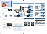
Page 22: ... 22 XS1 RM Y1011 2 3 SPEAKER REMOVAL 2 4 H1 BOARD REMOVAL 1 2 3 4 1 3 2 4 ...

Page 23: ... 23 XS1 RM Y1011 2 5 H2 BOARD REMOVAL 2 6 H3 BOARD REMOVAL 4 1 3 2 2 1 ...

Page 24: ... 24 XS1 RM Y1011 2 7 H4 BOARD REMOVAL 2 8 HMP BOARD COVER REMOVAL 2 1 2 1 ...

Page 25: ... 25 XS1 RM Y1011 2 9 U1 BOARD REMOVAL 2 10 APS 202 BOARD REMOVAL 2 1 2 1 ...

Page 26: ...ard Color Bar 0 525V ȑ62 BLUE output 0 000V 0ȑ6 one line A B C D SECTION 3 SET UP ADJUSTMENTS 3 1 CVBS PAL System Adjustment CVBS YC PAL SECAM NTSC RGB YUV 15K System adjustment CVBS PAL System adjustment White bar RED 216 3 A White bar BLUE 216 3 A 1 Input CVBS PAL Color Bar signal into AV1 as shown on Figure 1 Black bar RED 16 3 D EBU Standard Color Bar 100 Luma 75 Chroma Black bar BLUE 16 3 D V...

Page 27: ...BU Standard Color Bar 0 525V ȑ62 BLUE output 0 000V 0ȑ6 one line A B C D CVBS YC PAL SECAM NTSC RGB YUV 15K System adjustment CVBS SECAM System adjustment White bar RED 216 3 A White bar BLUE 216 3 A 1 Input CVBS SECAM Color Bar signal into AV1 as shown on Figure 1 Black bar RED 16 3 D EBU Standard Color Bar 100 Luma 75 Chroma Black bar BLUE 16 3 D VG828 ASTRO Pattern No XXX OPT 2 No F Red bar RED...

Page 28: ... SECAM EBU Standard Color Bar 0 525V ȑ62 BLUE output 0 000V 0ȑ6 one line A B C D CVBS YC PAL SECAM NTSC RGB YUV 15K System adjustment YC NTSC System adjustment White bar RED 216 3 A White bar BLUE 216 3 A 1 Input YC NTSC Color Bar signal into AV3 as shown on Figure 1 Black bar RED 16 3 D EBU Standard Color Bar 100 Luma 75 Chroma Black bar BLUE 16 3 D VG828 ASTRO Pattern No XXX OPT 2 No F Red bar R...

Page 29: ...igure 1 YUV EBU Standard Color Bar 0 525V ȑ62 BLUE output 0 000V 0ȑ6 one line A B C D CVBS YC PAL SECAM NTSC RGB YUV 15K System adjustment RGB System adjustment White bar RED 216 3 A White bar BLUE 216 3 A 1 Input RGB Color Bar signal into AV1 as shown on Figure 1 Black bar RED 16 3 D EBU Standard Color Bar 100 Luma 75 Chroma Black bar BLUE 16 3 D VG828 ASTRO Pattern No XXX OPT 2 No F Red bar RED ...

Page 30: ...ite Balance Adjustment Adjustment of W B With internal white signal Tool Measuring Instrument Component 1 Turn on the main power of XS1 CS 1000 Minolta 2 Execute the MID_H8_ServiceControl xls 3 H8_INIT SVC_FLAG RGBD 3 4 Adjust W B of warm Standard 8400k 27MPCD Color tone set to warm X 0 2943 0 003 H8_INIT SVC_WB RRTO warm set to FF Y 0 2840 0 003 1 H8_INIT SVC_WB GRTO warm 1 H8_INIT SVC_WB BRTO wa...

Page 31: ...ND PROCESSOR 3 23 10 18 SP PROT Q6015 Q6016 Q6017 SDA SCL SDA SCL X6007 6 SP R SP L OUT 1 OUT 2 14V IC6003 L R AMP MUTE SP PROT AUDIO CLOCK 10 IC6002 DIVIDER 11 16 9 5 1 IC6018 2 I P AND GATE 4 60 2 IC6000 PLL MSP TO AKM 4 3 16 IC6017 8 DIVIDER 10 5 11 4 IC6010 CLK LEVEL SHIFTER 2 SWITCH Q6014 AKM CLK FIN B VCO OUT 5 FIN A VDD AMPLIFIER SWITCH Q6070 Q6071 BUFFER AMP Q6002 Q6003 Q6064 BUFFER AMP Q6...

Page 32: ...L OUT 3 R OUT 3 CVBS TUN L TUN R TUN V IN 3 Y IN 3 C IN 3 L IN 3 R IN 3 MODE 3 AV LINK 2 AV LINK 2 V IN 1 MODE 1 L IN 1 R IN 1 U SEL CVBS MAIN Y SEL V SEL FSW SEL H SEL V SEL Y MAIN C MAIN CB SEL Y SEL CR SEL FSW OUT H SEL V SEL RESET CD UP SW DSP RDY SO DSP SI DSP SCLK RQ RESET DSP CS RESET SYS RS232 SIRCS 3 3V MS L SDA SCL MS R CS SDA SCL CN6002 CN6015 TO A3 BOARD 3 3V STBY S6201 BUFFER Q6020 SE...

Page 33: ... MARKED AS XX ARE NOT FITTED TO THIS MODEL XX SWITCH TO A3 BOARD CN4603 3 4 1 2 BLK 4P J9601 L R V J9602 J9600 UDZS TE17 12B D9600 UDZS TE17 12B D9601 UDZS TE17 12B D9602 UDZS TE17 12B D9603 UDZS TE17 12B D9604 UDZS TE17 12B D9605 UDZS TE17 12B D9607 UDZS TE17 12B D9606 UDZS TE17 12B D9608 UDZS TE17 12B D9609 UDZS TE17 12B D9610 UDZS TE17 12B D9611 UDZS TE17 12B D9612 VD9601 XX 1 2 3 4 5 6 7 8 9 1...

Page 34: ... F G H I J K L M N 1 2 3 4 5 6 7 8 9 10 11 O 34 H1 Printed Wiring Board Conductor Side A H1 Printed Wiring Board Conductor Side B H2 Printed Wiring Board Conductor Side A H2 Printed Wiring Board Conductor Side B ...

Page 35: ...ER 470 CN4601 TO A3 BOARD 1 2 3 GRY 3P CN9801 5V LOGO GND XX C9801 NSPW515BSA0 D9801 NSPW515BSA0 D9802 NSPW515BSA0 D9803 NSPW515BSA0 D9804 DTC114EUA T106 Q9801 DTC114EUA T106 Q9802 DTC114EUA T106 Q9803 DTC114EUA T106 Q9804 R9801 1 10W 100 R9802 1 10W 100 R9803 1 10W 100 R9804 1 10W 100 D9805 XX D9806 XX D9807 XX D9808 XX H4 XS1 COMPONENTS MARKED AS XX ARE NOT FITTED TO THIS MODEL H4 LED TO A3 BOAR...

Page 36: ... F G H I J K L M N 1 2 3 4 5 6 7 8 9 10 11 O 36 H4 Printed Wiring Board Conductor Side A H4 Printed Wiring Board Conductor Side B H3 Printed Wiring Board Conductor Side A H3 Printed Wiring Board Conductor Side B ...

Page 37: ...D E F G H I J K L M N 1 2 3 4 5 6 7 8 9 10 11 O 37 U1 Board Schematic Diagram Input Terminal AV SW Audio Page 1 6 COMPONENTS MARKED AS XX ARE NOT FITTED ON THIS MODEL INPUT TERMINAL AV SW AUDIO U1 XS1 U1 1 6 ...

Page 38: ...6V COMPONENTS MARKED AS XX ARE NOT FITTED ON THIS MODEL U1 XS1 U1 2 6 2 2 0 22 0 22 0 22 2 2K 0 2 2K 2 2K 2 2K 2 2K 2SC1623 L5L6 2SC4617R 2SA1774R 1UH 47 6 3V 0 22 100 6 3V 15K 0 15K 470 470 470 0 22 5 5V 2SA1774R 2SC3642A 2SC3624A 2 2K 2 2K 100 XX 220 75 50us div 50us div U1 2 6 Board Waveforms 420mVp p H 235mVp p H TP1 TP2 TP1 TP2 ...

Page 39: ...B C D E F G H I J K L M N 1 2 3 4 5 6 7 8 9 10 11 O 39 U1 Board Schematic Diagram Input Terminal AV SW Audio Page 3 6 COMPONENTS MARKED AS XX ARE NOT FITTED ON THIS MODEL U1 XS1 U1 3 6 0UH 0UH 0UH 0UH 100 ...

Page 40: ... K L M N 1 2 3 4 5 6 7 8 9 10 11 O 40 U1 Board Schematic Diagram Input Terminal AV SW Audio Page 4 6 COMPONENTS MARKED AS XX ARE NOT FITTED ON THIS MODEL TO H2 BOARD CN9601 JR6004 U1 XS1 U1 4 6 0 1 0 1 0 1 10P 8P 0 0 0 0 ...

Page 41: ...11 O 41 U1 Board Schematic Diagram Input Terminal AV SW Audio Page 5 6 0UH FB6037 C6042 2 2 50V 0UH AR5 E COMPONENTS MARKED AS XX ARE NOT FITTED ON THIS MODEL NJM2123M U1 XS1 U1 5 6 MA111 TX BTF EU611 100ns div U1 5 6 Board Waveform 2 9Vp p H TP1 TP1 ...

Page 42: ...A B C D E F G H I J K L M N 1 2 3 4 5 6 7 8 9 10 11 O 42 U1 Board Schematic Diagram Input Terminal AV SW Audio Page 6 6 COMPONENTS MARKED AS XX ARE NOT FITTED ON THIS MODEL U1 XS1 U1 6 6 0 1 0 1 100 ...

Page 43: ...0 7 5 0 9 5 8 5 0 5 3 0 2 1 4 1 8 5 3 4 0 6 1 5 7 3 6 3 8 3 3 1 3 2 9 5 5 4 9 6 1 6 0 8 3 0 7 4 1 0 3 0 6 4 4 1 7 0 7 1 5 1 7 0 7 1 5 1 0 0 6 C I 1 9 3 4 6 1 6 5 4 8 7 0 9 3 9 7 2 0 8 0 0 6 C I 3 1 5 4 1 8 0 0 4 0 7 3 9 3 4 0 3 8 2 8 5 2 4 4 3 4 0 4 9 3 7 5 5 4 4 8 0 8 4 5 4 8 3 5 7 9 8 1 9 6 8 5 8 5 2 9 4 0 4 0 0 6 C I 3 1 9 2 2 1 0 6 C I 4 2 1 5 9 8 7 8 0 1 5 0 5 8 3 5 4 1 1 5 0 1 9 0 9 1 5 2 5 ...

Page 44: ...1 0 6 D 9 B 4 3 0 6 D 7 B 0 6 0 6 D 9 C 1 0 5 6 D 8 F 6 3 0 6 Q 6 D 2 1 0 6 D 9 B 7 3 0 6 D 8 B 1 6 0 6 D 9 C 2 0 5 6 D 9 F 9 3 0 6 Q 9 G 3 1 0 6 D 9 B 8 3 0 6 D 8 D 2 6 0 6 D 8 D 3 0 5 6 D 4 F 0 4 0 6 Q 8 G 4 1 0 6 D 8 D 9 3 0 6 D 6 B 4 6 0 6 D 9 B 1 0 6 6 D 7 F 1 4 0 6 Q 8 G 5 1 0 6 D 9 D 0 4 0 6 D 7 D 5 6 0 6 D 9 B 2 0 6 6 D 8 G 2 7 0 6 Q 5 C 6 1 0 6 D 8 D 1 4 0 6 D 8 D 6 6 0 6 D 8 G 3 0 6 6 D ...

Page 45: ...BLANK2 2V5D 5VD GND D GND D 1uH L7014 1uH L7017 1uH L7015 1uH L7016 50V 2 2 C7041 XX C7044 XX C7043 XX C7047 XX C7045 6 3V 100 C7040 6 3V 100 C7042 6 3V 100 C7046 XX R7067 XX R7068 1 10W 100 R7015 1 10W 100 R7014 1 10W 100 R7043 CHIP 0 R7042 XX R7050 100 R7051 1 10W 100 R7052 UDZS TE17 12B D7003 UDZS TE17 12B D7002 XX R7065 XX R7066 RB7004 100 1 2 3 4 5 6 7 8 RB7003 100 1 2 3 4 5 6 7 8 RB7005 100 ...

Page 46: ...A B C D E F G H I J K L M N 1 2 3 4 5 6 7 8 9 10 11 O 46 N1 Printed Wiring Board Conductor Side A N1 Printed Wiring Board Conductor Side B ...

Page 47: ...TE85R1 IC TC7SZ08FU TE85R IC NJM2374AM TE2 IC TC7WH00FU TE12R IC TC7WHU04FU TE12R IC PQ20RX11J00H IC TAR5S30 TE85R IC TDA7490L IC UPC1093J 1 T 1 TOP VIEW 68 61 60 1 52 44 43 35 27 26 18 10 9 TOP VIEW REF ANODE CATHODE 1 16 17 32 1 100 25 26 50 51 75 76 TOP VIEW 1 8 16 9 5 6 7 1 2 3 4 IN GND OUT 2SA1037AK T146 R 2SA1162 G 2SC1623 L5L6 DTC144EE MSB709 RT1 E B C MA111 TX MM3Z12VT1 MM3Z3V9T1 MM3Z6V8T1...

Page 48: ...LECTOR YPbPr YCbCr BTA RGB YCbCr 41 IN2_1 42 IN2_2 43 IN2_3 44 IN2_H L1 45 IN2_V L2 46 IN2_L3 47 IN2_SW 1 IN3_1 2 IN3_2 3 IN3_3 4 IN3_H 5 IN3_V 7 IN4_1 8 IN4_2 9 IN4_3 10 IN4_H 11 15 16 13 14 IN4_V IN1 IN4 SELECTOR INPUT_SEL 2 SELSTB_1 1 SELSTB_2 1 DECL1_1 2 DECL2_1 2 DECL3_1 2 DECSW_1 1 DECL1_2 2 DECL2_2 2 DECL3_2 2 DECSW_2 1 EH 1 EV 1 HD_TC 1 HSEP_SEL 1 V_TC 2 MAT_OUT 2 3 STATE 1 YGAIN 4 CBGAIN ...

Page 49: ...NO DESCRIPTION REMARK 49 1 X 2021 896 2 COVER REAR 37 ASSY KDE P37XS1 2 X 2021 895 2 COVER REAR 42 ASSY KDE P42XS1 2 2 4 102 644 01 COVER 42 STAND BASE PAINTED 3 4 098 263 01 CAP 42 STAND 4 4 098 260 01 FRAME 42A STAND BASE 5 4 098 262 03 BRACKET 42 STAND BASE 6 4 098 259 02 PLATE 42 STAND BASE 7 4 098 261 01 FRAME 42B STAND BASE 8 4 098 264 01 CUSHION A 9 7 682 000 07 SCREW PSW M5X12 10 7 682 973...

Page 50: ... X 4042 973 1 BUTTON MULTI ASSY 62 4 098 110 01 GUIDE LIGHT MS 63 A 1606 623 A SPEAKER 37R ASSY KDE P37XS1 64 65 A 1606 608 A SPEAKER 42R ASSY KDE P42XS1 64 65 64 1 825 610 12 LOUDSPEAKER 5CM 65 1 825 609 11 LOUDSPEAKER 5 5X12CM 66 X 4042 983 1 FILTER GLASS BRACKET 37 ASSY KDE P37XS1 X 4042 968 1 FILTER GLASS BRACKET 42 ASSY KDE P42XS1 67 X 4042 760 3 BAR BOTTOM 37 ASSY KDE P37XS1 X 4042 754 3 BAR...

Page 51: ...01 BOX SPEAKER 37 REAR L PAINTED KDE P37XS1 4 102 214 01 BOX SPEAKER 42 REAR L PAINTED KDE P42XS1 82 X 4042 986 1 SPEAKER COVER 37L ASSY KDE P37XS1 X 4042 971 1 SPEAKER COVER 42L ASSY KDE P42XS1 83 A 1606 622 A SPEAKER 37L ASSY KDE P37XS1 64 65 A 1606 607 A SPEAKER 42L ASSY KDE P42XS1 64 65 84 4 098 215 02 MAIN FRM 37 ASSY KDE P37XS1 4 098 145 02 MAIN FRM 42 ASSY KDE P42XS1 85 4 098 094 03 LID CON...

Page 52: ...se items Parts indicated XX on the Schematic Diagram are not used in this model and therefore do not appear in the Parts List 52 H1 BOARD COMPLETE Parts List 53 H2 BOARD COMPLETE Parts List 53 N1 BOARD COMPLETE Parts List 53 H3 BOARD COMPLETE Parts List 55 H4 BOARD COMPLETE Parts List 56 U1 BOARD COMPLETE Parts List 56 MISCELLANEOUS 67 ACCESSORIES AND PACKAGING MATERIALS 67 REMOTE COMMANDER 67 Pag...

Page 53: ...ODE UDZS TE17 12B D9605 8 719 083 82 DIODE UDZS TE17 12B D9606 8 719 083 82 DIODE UDZS TE17 12B D9607 8 719 083 82 DIODE UDZS TE17 12B D9608 8 719 083 82 DIODE UDZS TE17 12B D9609 8 719 083 82 DIODE UDZS TE17 12B D9610 8 719 083 82 DIODE UDZS TE17 12B D9611 8 719 083 82 DIODE UDZS TE17 12B D9612 8 719 083 82 DIODE UDZS TE17 12B SOCKET J9600 1 568 267 11 JACK J9601 1 565 666 12 TERMINAL S 4P J9602 ...

Page 54: ...TE 0UH FB003 1 414 921 11 FERRITE 0UH FB004 1 414 921 11 FERRITE 0UH FB005 1 414 921 11 FERRITE 0UH FB006 1 414 921 11 FERRITE 0UH FB007 1 414 921 11 FERRITE 0UH FB008 1 414 921 11 FERRITE 0UH FB009 1 414 921 11 FERRITE 0UH FB010 1 414 921 11 FERRITE 0UH FB7006 1 469 835 21 FERRITE 0UH FB7010 1 469 835 21 FERRITE 0UH FB7011 1 414 760 21 FERRITE 0UH FB7012 1 469 835 21 FERRITE 0UH FB7013 1 469 835 ...

Page 55: ...63 1 216 864 11 SHORT CHIP 0 R7064 1 216 864 11 SHORT CHIP 0 R7069 1 216 811 11 METAL CHIP 150 5 1 10W R7071 1 216 864 11 SHORT CHIP 0 R7072 1 216 864 11 SHORT CHIP 0 R7075 1 216 864 11 SHORT CHIP 0 R7076 1 216 864 11 SHORT CHIP 0 R7077 1 216 864 11 SHORT CHIP 0 N1 H3 RESISTOR CHIP RB7000 1 233 576 11 RES CHIP NETWORK 100 3216 RB7001 1 233 576 11 RES CHIP NETWORK 100 3216 RB7002 1 233 576 11 RES C...

Page 56: ... 339 11 CERAMIC CHIP 0 1UF 10 00 50V C6092 1 115 185 11 CERAMIC CHIP 0 033UF 10 00 50V C6093 1 136 175 00 FILM 0 68UF 5 00 50V C6095 1 126 957 11 ELECT 0 22UF 20 00 50V C6096 1 136 175 00 FILM 0 68UF 5 00 50V C6098 1 163 133 00 CERAMIC CHIP 470PF 5 00 50V C6099 1 163 102 00 CERAMIC CHIP 24PF 5 00 50V C6100 1 126 941 11 ELECT 470UF 20 00 25V C6101 1 137 190 91 FILM 0 22UF 5 00 50V H3 H4 Q9705 8 729...

Page 57: ...V C6155 1 126 206 11 ELECT CHIP 100UF 20 00 6 3V C6156 1 127 715 91 CERAMIC CHIP 0 22UF 10 16V C6157 1 162 970 11 CERAMIC CHIP 0 01UF 10 00 25V C6158 1 127 573 11 CERAMIC CHIP 1UF 10 16V C6159 1 127 715 91 CERAMIC CHIP 0 22UF 10 16V C6160 1 127 715 91 CERAMIC CHIP 0 22UF 10 16V C6161 1 124 779 00 ELECT CHIP 10UF 20 00 16V C6162 1 162 970 11 CERAMIC CHIP 0 01UF 10 00 25V C6163 1 127 715 91 CERAMIC ...

Page 58: ...F 20 10V C6498 1 126 205 11 ELECT CHIP 47UF 20 00 6 3V C6499 1 164 388 91 CERAMIC CHIP 270PF 5 00 50V C6500 1 127 715 91 CERAMIC CHIP 0 22UF 10 16V C6250 1 127 715 91 CERAMIC CHIP 0 22UF 10 16V C6251 1 124 779 00 ELECT CHIP 10UF 20 00 16V C6252 1 124 779 00 ELECT CHIP 10UF 20 00 16V C6253 1 127 715 91 CERAMIC CHIP 0 22UF 10 16V C6254 1 124 779 00 ELECT CHIP 10UF 20 00 16V C6255 1 127 715 91 CERAMI...

Page 59: ... CHIP 0 22UF 10 16V C6504 1 127 715 91 CERAMIC CHIP 0 22UF 10 16V C6505 1 127 715 91 CERAMIC CHIP 0 22UF 10 16V C6506 1 126 197 11 ELECT CHIP 10UF 20 00 50V C6507 1 126 197 11 ELECT CHIP 10UF 20 00 50V C6508 1 162 970 11 CERAMIC CHIP 0 01UF 10 00 25V C6509 1 117 681 11 ELECT CHIP 100UF 20 00 16V C6510 1 162 966 11 CERAMIC CHIP 0 0022UF 10 00 50V C6511 1 162 966 11 CERAMIC CHIP 0 0022UF 10 00 50V C...

Page 60: ...DE MA111 TX D6093 8 719 312 92 DIODE RK14V1 D6094 8 719 312 92 DIODE RK14V1 D6095 8 719 081 97 DIODE MMDL914T1 D6096 8 719 081 97 DIODE MMDL914T1 D6097 8 719 404 50 DIODE MA111 TX D6301 8 719 081 98 DIODE MM3Z6V8T1 D6501 8 719 082 02 DIODE MM3Z3V9T1 D6502 8 719 082 02 DIODE MM3Z3V9T1 D6503 8 719 404 50 DIODE MA111 TX D6601 8 719 080 69 DIODE M1FS4 4063 D6602 8 719 080 69 DIODE M1FS4 4063 D6603 8 7...

Page 61: ...9 549 21 INDUCTOR 1UH L6017 1 469 549 21 INDUCTOR 1UH L6018 1 412 058 11 INDUCTOR 10UH L6019 1 469 549 21 INDUCTOR 1UH L6023 1 412 029 11 INDUCTOR 10UH L6025 1 216 864 11 SHORT CHIP 0 L6027 1 469 549 21 INDUCTOR 1UH L6028 1 469 549 21 INDUCTOR 1UH L6034 1 469 549 21 INDUCTOR 1UH L6035 1 469 549 21 INDUCTOR 1UH L6036 1 414 854 41 INDUCTOR 1MH L6037 1 412 030 11 INDUCTOR 22UH L6038 1 412 030 11 INDU...

Page 62: ...RES CHIP 680K 5 1 10W R6033 1 216 835 11 METAL CHIP 15K 5 1 10W R6034 1 216 117 00 RES CHIP 680K 5 1 10W Q6038 8 729 928 19 TRANSISTOR 2SA1774R Q6039 8 729 141 73 TRANSISTOR 2SC3624A T1L15L16 Q6040 8 729 141 73 TRANSISTOR 2SC3624A T1L15L16 Q6041 8 729 141 73 TRANSISTOR 2SC3624A T1L15L16 Q6042 8 729 928 19 TRANSISTOR 2SA1774R Q6043 8 729 120 28 TRANSISTOR 2SC1623 L5L6 Q6064 8 729 928 19 TRANSISTOR ...

Page 63: ...1 216 829 11 METAL CHIP 4 7K 5 1 10W R6125 1 216 817 11 METAL CHIP 470 5 1 10W R6126 1 216 829 11 METAL CHIP 4 7K 5 1 10W U1 R6127 1 216 830 11 METAL CHIP 5 6K 5 1 10W R6128 1 216 841 11 METAL CHIP 47K 5 1 10W R6129 1 216 813 11 METAL CHIP 220 5 1 10W R6130 1 216 813 11 METAL CHIP 220 5 1 10W R6131 1 216 813 11 METAL CHIP 220 5 1 10W R6132 1 216 813 11 METAL CHIP 220 5 1 10W R6133 1 216 795 11 MET...

Page 64: ...11 METAL CHIP 10K 5 1 10W R6230 1 216 821 11 METAL CHIP 1K 5 1 10W R6231 1 216 821 11 METAL CHIP 1K 5 1 10W R6232 1 216 833 11 METAL CHIP 10K 5 1 10W R6233 1 216 864 11 SHORT CHIP 0 R6234 1 216 825 11 METAL CHIP 2 2K 5 1 10W R6235 1 216 864 11 SHORT CHIP 0 R6236 1 216 825 11 METAL CHIP 2 2K 5 1 10W R6237 1 216 864 11 SHORT CHIP 0 R6238 1 216 825 11 METAL CHIP 2 2K 5 1 10W R6239 1 216 817 11 METAL ...

Page 65: ...2K 5 1 10W R6378 1 216 057 00 RES CHIP 2 2K 5 1 10W R6379 1 216 022 00 RES CHIP 75 5 1 10W R6380 1 216 834 11 METAL CHIP 12K 5 1 10W R6381 1 216 853 11 METAL CHIP 470K 5 1 10W R6382 1 216 841 11 METAL CHIP 47K 5 1 10W R6383 1 216 853 11 METAL CHIP 470K 5 1 10W R6384 1 216 841 11 METAL CHIP 47K 5 1 10W R6385 1 216 821 11 METAL CHIP 1K 5 1 10W R6386 1 216 821 11 METAL CHIP 1K 5 1 10W R6387 1 216 837...

Page 66: ... 5 1 10W R6653 1 216 864 11 SHORT CHIP 0 R6654 1 216 864 11 SHORT CHIP 0 R6657 1 216 809 11 METAL CHIP 100 5 1 10W R6658 1 216 809 11 METAL CHIP 100 5 1 10W R6659 1 216 809 11 METAL CHIP 100 5 1 10W R6660 1 216 809 11 METAL CHIP 100 5 1 10W R6661 1 216 829 11 METAL CHIP 4 7K 5 1 10W R6662 1 216 809 11 METAL CHIP 100 5 1 10W R6663 1 216 809 11 METAL CHIP 100 5 1 10W R6664 1 216 809 11 METAL CHIP 10...

Page 67: ...RK RESISTOR CHIP 100 RB6016 1 239 412 11 NETWORK RESISTOR CHIP 100 SWITCH S6201 1 572 921 11 SWITCH KEY BOARD TUNER TU6000 8 598 529 10 FRONTEND BTF EU611 VARISTOR VD6000 1 803 974 21 VARISTOR CHIP 1608 VD6001 1 803 974 21 VARISTOR CHIP 1608 VD6002 1 803 974 21 VARISTOR CHIP 1608 CRYSTAL X6003 1 781 922 21 VIBRATOR CERAMIC X6007 1 813 283 21 VIBRATOR CRYSTAL MISCELLANEOUS 1 758 986 21 GLASS OPTICA...

Page 68: ...re modules Please contact your local Sony Service organisation for the latest information Read restore and compare NVM contents via the I2C bus Acknowledge check of all I2C devices in the TV set Read Error Codes emulation of the Error Reader tool Remote Commander emulation User programmable Functional Check through Infrared Fast and documented Test Mode setting of all Sony TV chassis Partnumbers T...

Reviews: