SERVICE MANUAL
Sony Corporation
Home Audio Division
Published by Sony Techno Create Corporation
US Model
DVD PLAYER
9-879-748-03
2006E16-1
© 2006.05
SPECIFICATIONS
DVP-NW50
This Unit incorporates Dolby* Digital and Pro Logic surround and
the DTS** Digital Surround System.
* Manufactured under license from Dolby Laboratories.
“Dolby,” “Pro Logic,” and the double-D symbol are trademarks
of Dolby Laboratories.
** Manufactured under licence from Digital Theater System, Inc.
“DTS” and “DTS Digital Surround” are registered trademarks
of Digital Theater System, Inc.
Model Name Using Similar Mechanism
NEW
Mechanism Type
IDM-520DR
Laser
Signal format system
Audio section
Frequency response
Signal-to-noise ratio
Rated output power 1 kHz into 8 ohms THD: 3 %
Reference Output Power
(8ohms 1 kHz THD:3%)
(8ohms 30 Hz THD:3%)
Harmonic distortion
Wow and flutter
Tuner section
Frequency range
Signal-to-noise ratio
THD at 400 Hz
THD at 1 kHz
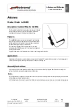
Antenna (aerial)
Antenna (aerial) terminals
Intermediate frequency
AM tuner section
Antenna (aerial)
Intermediate frequency
Semiconductor laser
CD:
λ
= 780 nm, DVD:
λ
= 650 nm
Emission duration: continuous
NTSC
20 Hz to 20 kHz (
±
1 dB)
95 dB
50 W + 50 W
FRONT: 50 W + 50 W
CENTER: 50 W
SURROUND: 50 W + 50 W
SUB WOOFER: 50 W
Less than 0.1 %
Less than detected value
(
±
0.001 % W PEAK)
87.5 Hz to 108 kHz (100 kHz step)
530 kHz to 1710 kHz (10 kHz step)
54 dB
76 dB (MONO)
70 dB (STEREO)
0.5 %
0.3 % (MONO)
0.5 % (STEREO)
FM wire antenna (aerial)
75 ohms, unbalanced
10.7 MHz
AM loop antenna (aerial)
450 kHz
Video section
Composite video out:
S1 video out:
General
DC power consumption:
Operating temperature:
Dimensions:
Mass:
Supplied accessories :
• Remote commander (remote)(RM-ANU001)(1)
• Wall mounting bracket (1)
• Wall stopper (4)
• TEMPLATE (1)
• Plug-in 4P terminal (for speakers)(3)
• Plug-in 6P terminal (for AC power unit)(1)
• Screws for fixing the Unit to the wall mounting bracket (Short)(4)
• Screws for wall stopper (long)(4)
• Screws for AM antenna (2)
• AM loop antenna (aerial)(1)
• R6 (size-AA) battery (2)
• Utility for In-Wall Unit CD-ROM (1)
• User’s manual (1)
• Installer’s manual (1)
Design and specifications are subject to change without notice.
1 Vp-p 75 ohms
Y: 1 Vp-p 75 ohms
V: 0.286 Vp-p 75 ohms
DC 29.5 V/1 A
DC 29.5 V/1 A
DC 14 V/1.5 A
0 ˚C to 40 ˚C (– 32 ˚F to 104 ˚F)
230
×
266
×
104 mm
(9
1
/
8
×
10
1
/
2
×
4
1
/
8
inches)
(w/h/d)
2.7 kg (5 lbs 15 oz)