background image

1

Model Name Using Similar Mechanism

D-NE509

CD Mechanism Type

CDM-3325ER2

Optical Pick-up Name

DAX-25E

SERVICE MANUAL

US Model

Canadian Model

D-NE500/NE506CK

E Model

D-NE500

D-NE500/NE506CK

PORTABLE CD PLAYER

CD player
System

Compact disc digital audio system

Laser diode properties

Material: GaAlAs
Wavelength: 

λ

 = 770 - 800 nm

Emission duration: Continuous
Laser output: Less than 44.6 

µ

W

(This output is the value measured at a distance
of 200 mm from the objective lens surface on
the optical pick-up block with 7 mm aperture.)

D-A conversion

1-bit quartz time-axis control

Frequency response

20 - 20 000 Hz     dB (measured by JEITA)

Output (at 3 V input level)

Headphones (stereo minijack)
   Approx. 5 mW + Approx. 5 mW at 16 

SPECIFICATIONS

General
Power requirements

• LR6 (size AA) battery: 1.5 V DC 

×

 1

• AC power adaptor (DC IN 3 V jack):

120 V, 60 Hz

Battery life*1 (approx. hours)

When you use the CD player on a flat and stable
surface.
When LIGHT mode and SOUND mode are set to
“OFF.”
Playing time varies depending on how the CD
player is used.

US, CND model:

When using one Sony alkaline battery LR6
(SG) (produced in Japan)

G-PROTECTION

“G-PRO 1”

“G-PRO 2”

Audio CD

33

28

ATRAC CD

*

2

60

60

MP3 CD

*

3

45

45

*1 Measured value by the standard of JEITA

(Japan Electronics and Information Technology
Industries Association)

*2 Recorded at 48 kbps
*3 Recorded at 128 kbps

Operating temperature

5

°

C - 35

°

C (41

°

F - 95

°

F)

Dimensions (w/h/d) (excluding projecting
parts and controls)

Approx. 129 

×

 27.5 

×

 140.1 mm

(5

 1 ⁄8


×

 1

 1 ⁄8


×

 5

 5 ⁄8

 in.)

Mass (excluding accessories)

Approx. 188 g (6.7 oz.)

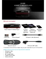
Supplied accessories

AC power adaptor (1) (for except D-NE500:
   US, except D-NE506CK: CND)
Remote control (1)
Rotary commander (1) (for D-NE506CK)
Car battery cord (1) (for D-NE506CK)
Car connecting pack (1) (for D-NE506CK)
Carrying case (1)
CD-ROM (SonicStage Ver. 2.0) (1)
User’s guide for SonicStage Ver. 2.0 (1)
Headphones (1) (for US model)
Earphones (1) (for other models)

US and foreign patents licensed from Dolby
Laboratories.

Design and specifications are subject to change
without notice.

• Abbreviation

CND : Canadian model
E92 : AC 120V area in E model
MX : Mexican model

Ver 1.1  2004. 10

9-877-555-02

2004J04-1

© 2004.10

Sony Corporation

Personal Audio Company

Published by Sony Engineering Corporation

+1
–2

Photo: D-NE500

Summary of Contents for CD Walkman D-NE500

Page 1: ...CD player is used US CND model When using one Sony alkaline battery LR6 SG produced in Japan G PROTECTION G PRO 1 G PRO 2 Audio CD 33 28 ATRAC CD 2 60 60 MP3 CD 3 45 45 1 Measured value by the standard of JEITA Japan Electronics and Information Technology Industries Association 2 Recorded at 48 kbps 3 Recorded at 128 kbps Operating temperature 5 C 35 C 41 F 95 F Dimensions w h d excluding projecti...

Page 2: ...ed to the solder joint for a slightly longer time Soldering irons using a temperature regulator should be set to about 350 C Caution The printed pattern copper foil may peel away if the heated tip is applied for too long so be careful Strong viscosity Unleaded solder is more viscous sticky less prone to flow than ordinary solder so use caution not to let solder bridges occur such as on IC pins etc...

Page 3: ...ted Wiring Boards and Schematic Diagrams 15 5 3 Waveforms 15 5 4 Block Diagram CD Section 16 5 5 Block Diagram Power Supply Section 17 5 6 Printed Wiring Board Main Section 18 5 7 Schematic Diagram Main Section 1 2 20 5 8 Schematic Diagram Main Section 2 2 21 5 9 Printed Wiring Board Switch Section 22 5 10 Schematic Diagram Switch Section 23 5 11 IC Block Diagrams 24 6 EXPLODED VIEWS 6 1 Upper Lid...

Page 4: ...ation of the equipment emission of the laser diode is prohibited unless the upper lid is closed while turning ON the S803 push switch type The following two checking methods for the laser diode are operable Method Emission of the laser diode is visually checked 1 Open the upper lid 2 With a disc not set turn on the S803 with a screwdriver having a thin tip Note Do not push the detection lever stro...

Page 5: ...er is playing 4 Battery indication 31 Roughly shows the remaining power of the battery If flashes the battery is depleted 5 Play list indication For MP3 CD only 6 Group indication For ATRAC CD MP3 CD only 7 Play mode indication Shows various play modes such as single play shuffle play and program play shows repeat play 8 SOUND indication Shows the SOUND setting which has been selected on the menu ...

Page 6: ...MBLY The equipment can be removed using the following procedure 3 1 UPPER LID ASSY Page 7 3 2 CABINET MIDDLE ASSY Page 7 SET 3 3 MAIN BOARD MD ASSY Page 8 3 4 SLED MOTOR ASSY M602 OPTICAL PICK UP DAX 25E TURNTABLE MOTOR ASSY M601 Page 8 ...

Page 7: ...y procedure in the numerical order given 3 1 UPPER LID ASSY 3 2 CABINET MIDDLE ASSY 1 screw 2 bracket hinge R upper lid assy spring upper lid 5 7 6 4 bracket hinge L 3 screw 1 three screws 4 2 three screws 5 cabinet middle assy 3 screw two claws ...

Page 8: ...M601 Note When installing fit the knob HOLD and S802 7 MAIN board claw knob hold S802 cabinet lower assy 5 MD ASSY 2 CN603 1 CN602 3 CN602 8 CN802 4 6 3 5 4 sled motor assy M901 1 three screws B1 7x4 Chassis 8 three screws B1 7x4 9 turntable motor assy M902 6 optical pick up DAX 25E 7 standard shaft 2 gear cover ...

Page 9: ...nts are done automatically in this set In case of operation check confirm that focus bias FOCUS BIAS CHECK 1 Connect the oscilloscope between TP610 RF and GND on main board 2 Insert the disc YEDS 18 Part No 3 702 101 01 3 Press the N X button 4 Confirm that the oscilloscope waveform is as shown in the figure below eye pattern A good eye pattern means that the diamond shape in the center of the wav...

Page 10: ...tem controller L reset 29 PWMI I Spindle motor external control signal input terminal Not used 30 XQOK I Subcode Q OK signal input terminal Not used 31 XWRE I D RAM write enable signal input terminal Not used 32 R8M O System clock output to the system controller 33 VSS0 Ground terminal digital system 34 SQCK I SQSO readout clock input terminal Not used 35 SCLK I SENS serial data read clock input t...

Page 11: ...log system 80 ASY_O O EFM full swing output terminal 81 ASY_I I Asymmetry comparator voltage input terminal 82 BIAS I Asymmetry circuit constant current input terminal 83 AVDD3 Power supply terminal analog system 84 RFAC I EFM signal input from the optical pick up 85 AVDD0 Power supply terminal analog system 86 IGEN I Stabilized current input for operational amplifiers 87 AVSS0 Ground terminal ana...

Page 12: ...tput terminal 109 PCMD_I I Serial data input terminal 110 BCK_O O Bit clock 2 8224 MHz output terminal 111 BCK_I I Bit clock 2 8224 MHz input terminal 112 DVDD Power supply terminal for D RAM interface 113 to 117 A3 to A0 A10 O Address signal output to the D RAM 118 to 120 A11 to A13 O Address signal output terminal to the D RAM Not used ...

Page 13: ...ntroller 22 DTS_SDTI I Serial data input from the DTS controller 23 DTS_SCK O Clock output to the DTS controller 24 AM0_I I Not used fixed at H 25 VCPU Power supply terminal 26 XOUT O Clock output not used 27 GND Ground terminal 28 XIN I Clock input 29 AM1_I I Not used fixed at H 30 XRESET_I I Reset signal input L reset 31 TSB I O Data input output from to the remote control 32 XWAKE_O O Wake sign...

Page 14: ... off signal output 78 BOOT I BOOT signal input 79 XBAT1CELL I I Not used fixed at L 80 NC Not used open 81 XCEX_I I Not used open 82 DISPLAY_TYPE_I I Not used fixed at L 83 MSCK0_O O Clock signal output to the DSP IC601 and the power control IC401 84 MSDTO0_O O Serial data output to the DSP IC601 and the power control IC401 85 MSDTI0_I I SENS signal input from the DSP IC601 86 SCOR_I I SCOR signal...

Page 15: ...easure Voltages are taken with aVOM Input impedance 10 MΩ Voltage variations may be noted due to normal produc tion tolerances Waveforms are taken with a oscilloscope Voltage variations may be noted due to normal produc tion tolerances Circled numbers refer to waveforms Signal path F FM f AM J CD Abbreviation CND Canadian model E92 AC 120V area in E model MX Mexican model Abbreviation CND Canadian...

Page 16: ...69 28 25 87 XLATO_O 88 XSOE_O 86 SCOR_I 28 XIN 53 GFS_I 4 XRST_O 7 AMUTE_O 30 XRESET_I VCPU DO DI XSK XCS RESET TESET CONNECTOR CN801 IC802 EEPROM 78 BOOT 22 23 21 DTS_SDTO DTS_SDTI DTS_SCK 20 SDIN_I 17 SDXLAT_O 19 SDOUT_O 18 SDCLK_O 67 EEP_CS_O 11 REQ_I 66 WAKEUP_K_O 60 AT3_MP3_V_O 8M28 RST30 BOOT TXD21 RXD22 TCK23 2 3 4 1 RF3 T3 37 SCS0 42 SIO 41 SO0 40 SCK0 RF0 8 EXTAL X701 22MHz XTAL 38 34 30 ...

Page 17: ... HP_PWRSW AD RMKEY JOGKEY_I FAVKEY_I AD KEY1 AD KEY2 RE1_I RE2_I XLED1_O XLED2_O XRD_O XWR_O LCD XRST_O LCD_AO AD0 AD7 90 HOLD_I 40 VDSW19 19 J401 DC IN 3V BATTERY 3V Q801 Q801 PW IC301 HEADPHONE AMP IC801 2 2 SYSTEM CONTROL IC401 2 2 POWER SUPPLY IN L OUT L CD L LRMU BEEP I L 13 4 BEEP O L PW SW 3 16 99 77 36 96 97 14 15 75 76 71 72 73 69 18 MUTE SW 17 BEEP_O 6 44 51 POWER SWITCH IC701 POWER SWIT...

Page 18: ...27 C419 L405 L409 L404 R456 R450 R701 R424 R422 R447 R448 C446 R425 R426 C455 C456 D306 D308 D101 D305 J301 J301 i C633 15 1 Q403 Q404 G S G D S D G S G D S D Q405 E C B VDR302 VDR604 VDR608 VDR601 C602 CN604 C607 C627 R419 R427 C422 C451 R304 C306 L302 L604 OPTICAL PICK UP BLOCK DAX 25E 1 861 077 11 11 BLK M602 SLED MOTOR M601 SPINDLE MOTOR RED CN602 RED GRY PNK BLK 5 6 PRINTED WIRING BOARD MAIN ...

Page 19: ...48 TP646 TP647 TP645 TP420 TP404 C808 C801 C802 C703 R708 C716 C718 C405 R725 VDR610 TP406 TP405 FB603 FB602 FB301 C104 C204 C428 R420 D401 C432 C433 C445 FB403 C454 C440 C448 R409 R457 VDR401 VDR402 C401 VDR606 R441 D406 R644 C814 C610 C623 FB606 C609 VDR603 C625 FB402 FB401 R408 C704 C702 R717 X701 C712 C714 IC801 CN801 C811 R837 R827 R828 R829 R303 TP834 TP832 TP830 TP828 TP826 R713 R705 C708 C...

Page 20: ...702 R713 C702 R703 R704 R710 C703 R708 TP703 TP704 TP705 TP706 R707 CN603 CN602 TP605 TP606 R706 R701 C711 IC301 C204 C104 R202 R204 C205 R102 R104 C105 C206 C106 C301 C304 R308 C309 C305 C307 R305 C302 R311 C306 R304 R103 R203 L302 TP201 TP101 R631 C633 C602 M602 M601 C617 FB606 VDR608 FB605 C627 R640 C615 C616 C621 TP701 R452 C452 IC701 C706 C708 TP714 C713 C718 TP713 TP711 TP709 C715 C714 C710 ...

Page 21: ...101 D306 D305 TP303 TP301 TP302 C311 R314 R315 FB301 FB302 VDR302 C815 S803 S802 TP813 R857 CN801 IC802 TP811 C814 R801 C810 C807 C809 R814 TP804 R818 R819 C812 R840 R834 VDR802 R832 R828 R839 R831 D801 R836 R835 R824 R841 R827 TP819 TP818 TP805 SL805 TP803 R845 TP815 R810 TP817 TP816 C808 C801 C802 C804 C805 C806 R802 R803 TP806 R303 TP202 TP102 R812 C803 C816 R829 R411 C457 IC401 R858 R826 Q803 ...

Page 22: ...AY MENU S2002 S2005 S2005 VOL S2001 JOG S2003 OPR D2001 S2004 S2006 S2003 TP2006 R2025 R2018 R2017 R2024 R2007 R2032 R2029 R2010 R2027 R2012 R2014 R2022 R2026 R2015 R2021 R2013 R2006 R2020 R2011 R2038 R2009 C2001 R2001 R2004 R2003 MAIN BOARD CN802 R2036 R2016 R2005 TP2005 TP2003 TP2004 1 861 118 11 11 SWITCH BOARD A x NX D2001 5 9 PRINTED WIRING BOARD SWITCH SECTION Uses unleaded solder Page 19 ...

Page 23: ...03 R2007 S2006 S2005 S2004 S2003 R2006 S2002 R2010 R2029 R2001 R2005 TP2006 S2001 TP2008 R2038 R2032 R2011 R2027 R2018 R2022 R2017 R2031 R2026 R2015 R2025 R2014 R2024 R2020 R2013 R2012 R2016 R2009 R2021 TP2005 TP2003 TP2004 TP2007 5 10 SCHEMATIC DIAGRAM SWITCH SECTION Page 20 ...

Page 24: ...I0 PC1 SO0 VDIOCD2 PC0 SCK0 PF3 T3 PF2 EC2 INT4 PF1 T1 OF0 EC0 INT3 RST KCS VDIO1 KDO KDI KRB DVDD1 DVSS3 AVDPLL AVSPLL AVSSOSC AVDMO EXTAL XTAL XIN OSCSEL KCLK INTERRUPT CONTROLLER 8BIT TIMER CH6 8BIT TIMER CH7 8BIT TIMER CH4 8BIT TIMER CH5 8BIT TIMER COUNTER CH2 8BIT TIME 8BIT TIMER COUNTER CH0 8BIT TIMER CH1 17 18 19 20 21 22 23 24 25 26 27 28 29 30 31 32 42 41 40 39 38 37 36 35 34 33 44 43 PE3...

Page 25: ...al for safety Replace only with part number specified Les composants identifiés par une marque 0 sont critiques pour la sécurité Ne les remplacer que par une piéce portant le numéro spécifié 1 X 3385 073 1 LID ASSY S UPPER SILVER SILVER NE500 1 X 3385 074 1 LID ASSY B UPPER BLACK BLACK NE500 1 X 3385 075 1 LID ASSY B UPPER BLACK BLACK NE506CK 2 3 261 330 01 KNOB DIAL 3 3 261 333 01 HOLDER KNOB 4 3...

Page 26: ...1 KNOB HOLD SILVER SILVER 52 3 261 317 11 KNOB HOLD BLACK BLACK 53 3 261 320 01 SPRING UPPER LID 54 X 3385 135 1 MAIN BOARD COMPLETE 55 3 261 318 01 BOARD TERMINAL BATTERY 56 3 261 319 01 BOARD TERMINAL BATTERY 57 3 245 331 02 INSULATOR 58 3 258 918 31 LID BATTERY CASE 59 3 254 070 11 SCREW 60 3 261 321 01 CABINET MIDDLE 61 3 258 915 01 CLAW R LOCK 62 3 261 322 01 SPRING TORSION 63 3 258 914 01 CL...

Page 27: ...placer que par une piéce portant le numéro spécifié 101 3 318 203 61 SCREW B1 7X4 TAPPING 102 3 221 474 01 SPRING SLED 103 3 221 472 02 CHASSIS 104 A 3331 663 A SCREW FEED ASSY 105 3 221 473 01 COVER GEAR 106 3 221 268 01 GEAR B 0107 X 3380 950 1 DAX 25E RP ASSY 108 3 221 475 01 SHAFT STANDARD 109 3 222 298 01 RACK 110 3 222 299 01 SPRING RACK RETAINER 111 3 348 998 31 SCREW M1 4X2 5 TAPPING PAN M...

Page 28: ...AMIC CHIP 0 1uF 10 10V C414 1 107 820 11 CERAMIC CHIP 0 1uF 16V C415 1 107 820 11 CERAMIC CHIP 0 1uF 16V C416 1 131 862 11 TANTAL CHIP 47uF 20 4V C417 1 107 820 11 CERAMIC CHIP 0 1uF 16V C418 1 137 739 11 TANTAL CHIP 22uF 20 6 3V C419 1 107 820 11 CERAMIC CHIP 0 1uF 16V C420 1 131 862 11 TANTAL CHIP 47uF 20 4V C421 1 128 964 11 TANTAL CHIP 100uF 20 6 3V C422 1 107 820 11 CERAMIC CHIP 0 1uF 16V C42...

Page 29: ... C816 1 107 820 11 CERAMIC CHIP 0 1uF 16V CONNECTOR CN602 1 785 877 21 HOUSING CONNECTOR 4P CN603 1 784 342 21 HOUSING CONNECTOR 2P CN604 1 818 127 21 CONNECTOR FFC FPC 15P ZIF L CN802 1 818 064 21 CONNECTOR FFC FPC ZIF 24P DIODE D101 8 719 422 37 DIODE MA8051 D202 8 719 422 37 DIODE MA8051 D305 8 719 422 37 DIODE MA8051 D306 8 719 422 37 DIODE MA8051 D308 8 719 422 37 DIODE MA8051 D401 6 500 483 ...

Page 30: ...RT CHIP 0 R434 1 218 965 11 RES CHIP 10K 5 1 16W R436 1 218 965 11 RES CHIP 10K 5 1 16W R437 1 218 961 11 RES CHIP 4 7K 5 1 16W R438 1 218 969 11 RES CHIP 22K 5 1 16W R439 1 220 804 11 RES CHIP 2 2M 5 1 16W R440 1 218 965 11 RES CHIP 10K 5 1 16W R441 1 216 864 11 METAL CHIP 0 5 1 10W R442 1 218 965 11 RES CHIP 10K 5 1 16W R444 1 218 989 11 RES CHIP 1M 5 1 16W R445 1 218 973 11 RES CHIP 47K 5 1 16W...

Page 31: ...CH PUSH 1 KEY OPEN CLOSE VARISTOR VDR302 1 801 862 11 VARISTOR CHIP 1608 VDR401 1 801 862 11 VARISTOR CHIP 1608 VDR402 1 801 862 11 VARISTOR CHIP 1608 VDR601 1 801 862 11 VARISTOR CHIP 1608 VDR602 1 801 862 11 VARISTOR CHIP 1608 VDR603 1 801 862 11 VARISTOR CHIP 1608 VDR604 1 801 862 11 VARISTOR CHIP 1608 VDR606 1 801 862 11 VARISTOR CHIP 1608 VDR608 1 801 862 11 VARISTOR CHIP 1608 VDR609 1 801 86...

Page 32: ... EXPLANATION CARD NE500 MX 3 262 155 01 EXPLANATION CARD NE506CK US 3 266 166 11 MANUAL INSTRUCTION SONICSTAGE Ver 2 0 ENGLISH US CND E92 3 266 166 21 MANUAL INSTRUCTION SONICSTAGE Ver 2 0 SPANISH PORTUGUESE FRENCH CND E92 MX 3 266 356 11 MANUAL INSTRUCTION ENGLISH NE500 US CND E92 3 266 356 21 MANUAL INSTRUCTION SPANISH PORTUGUESE NE500 E92 MX 3 266 356 31 MANUAL INSTRUCTION FRENCH NE500 CND 3 26...

Page 33: ...33 D NE500 NE506CK MEMO ...

Page 34: ...ng the version allows you to jump to the revised page Also clicking the version at the upper on the revised page allows you to jump to the next revised page Ver Date Description of Revision 1 0 2004 01 New 1 1 2004 10 Change of IC801 SPM 04132 ...

Reviews: