background image

Rev 1.1 11/14

Copyright © 2013 by Silicon Laboratories

SiM3L1xx


SiM3L1xx

High-Performance, Low-Power, 32-Bit Precision32™ 

MCU Family with up to 256 kB of Flash

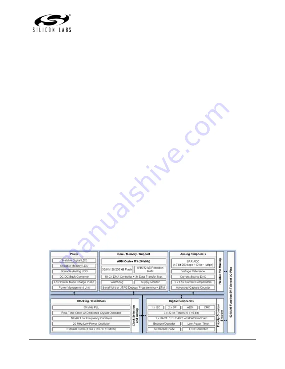
32-bit ARM Cortex-M3 CPU

-

50

  MHz maximum frequency

-

Single-cycle multiplication, hardware division support

-

Nested vectored interrupt control (NVIC) with 8 priority levels

Memory

-

32–256


kB flash, in-system programmable

-

8–32


kB SRAM with configurable low power retention

Clock Sources

-

Internal oscillator with PLL: 23–50


MHz

-

Low power internal oscillator: 20


MHz

-

Low frequency internal oscillator (LFO): 16.4


kHz

-

External real-time clock (RTC) crystal oscillator

-

External oscillator: Crystal, RC, C, CMOS clock

Power Management

-

Three adjustable low drop-out (LDO) regulators

-

Power-on reset circuit and brownout detectors

-

DC-DC buck converter allows dynamic voltage scaling for 
maximum


efficiency (250 mW output)

-

Multiple power modes supported for low power optimization

Low Power Features

-

75

  nA typical current in Power Mode 8

-

Low-current RTC (180


nA from LFO, 300


nA from crystal)

-

μ

s wakeup, register state retention and no reset required from 

lowest power mode

-

175


μ

A/MHz at 3.6


V executing from flash

-

140


μ

A/MHz at 3.6


V executing from SRAM

-

Specialized on-chip charge pump reduces power consumption

-

Process/Voltage/Temperature (PVT) Monitor

5 V Tolerant Flexible I/O

-

Up to 62 contiguous 5 V tolerant GPIO with one priority cross-
bar providing flexibility in pin assignments

Temperature Range: –40 to +85


°C

Supply Voltage: 1.8 to 3.8


V

Analog Peripherals

-

12-Bit Analog-to-Digital Converter: Up to 250


ksps 12-bit mode 

or 1


Msps 10-bit mode

-

10-Bit Current-mode Digital-to-Analog Converter

-

2 x Low-current comparators

Digital and Communication Peripherals

-

1 x USART with IrDA and ISO7816 Smartcard support

-

1 x UART that operates in low power mode

-

2 x SPIs, 1 x I2C, 16/32-bit CRC

-

128/192/256-bit Hardware AES Encryption

-

Encoder/Decoder: Manchester and Three-out-of-Six

-

Integrated LCD Controller: up to 160 segments (40x4), auto-
contrast and low power operation

Timers/Counters

-

3 x 32-bit or 6 x 16-bit timers with capture/compare

-

16-bit, 6-channel counter with capture/compare/PWM and 
dead-time controller with differential outputs

-

16-bit low power timer/advanced capture counter operational in 
the lowest power mode

-

32-bit real time clock (RTC) with multiple alarms

-

Watchdog timer

-

Low power mode advanced capture counter (ACCTR)

Data Transfer Peripherals

-

10-Channel DMA Controller

-

3 Channel Data Transfer Manager manages complex DMA 
transfers without core intervention

On-Chip Debugging

-

Serial wire debug (SWD) with serial wire viewer (SWV) or JTAG 
(no boundary scan) allow debug and programming

-

Cortex-M3 embedded trace macrocell (ETM)

Package Options

-

QFN options: 40-pin (6 x 6


mm), 64-pin (9 x 9


mm)

-

TQFP options: 64-pin (10 x 10


mm), 80-pin (12 x 12


mm)

Summary of Contents for SiM3L1xx

Page 1: ...V Tolerant Flexible I O Up to 62 contiguous 5 V tolerant GPIO with one priority cross bar providing flexibility in pin assignments Temperature Range 40 to 85 C Supply Voltage 1 8 to 3 8 V Analog Peripherals 12 Bit Analog to Digital Converter Up to 250 ksps 12 bit mode or 1 Msps 10 bit mode 10 Bit Current mode Digital to Analog Converter 2 x Low current comparators Digital and Communication Periphe...

Page 2: ...2 Rev 1 1 ...

Page 3: ...cess Voltage Temperature Monitor TIMER2 and PVTOSC0 38 4 2 I O 39 4 2 1 General Features 39 4 2 2 Crossbar 39 4 3 Clocking 40 4 3 1 PLL PLL0 41 4 3 2 Low Power Oscillator LPOSC0 41 4 3 3 Low Frequency Oscillator LFOSC0 41 4 3 4 External Oscillators EXTOSC0 41 4 4 Integrated LCD Controller LCD0 42 4 5 Data Peripherals 43 4 5 1 10 Channel DMA Controller 43 4 5 2 Data Transfer Managers DTM0 DTM1 DTM2...

Page 4: ... 4 TQFP 80 Package Specifications 74 6 4 1 TQFP 80 Solder Mask Design 77 6 4 2 TQFP 80 Stencil Design 77 6 4 3 TQFP 80 Card Assembly 77 6 5 QFN 64 Package Specifications 78 6 5 1 QFN 64 Solder Mask Design 80 6 5 2 QFN 64 Stencil Design 80 6 5 3 QFN 64 Card Assembly 80 6 6 TQFP 64 Package Specifications 81 6 6 1 TQFP 64 Solder Mask Design 84 6 6 2 TQFP 64 Stencil Design 84 6 6 3 TQFP 64 Card Assemb...

Page 5: ...ies Hardware Access Layer HAL API provides C language functions to modify and read each bit in the SiM3L1xx devices This description can be found in the SiM3xxxx HAL API Reference Manual 1 1 3 ARM Cortex M3 Reference Manual The ARM specific features like the Nested Vectored Interrupt Controller are described in the ARM Cortex M3 reference documentation The online reference manual can be found here...

Page 6: ...Diagram with DC DC Converter Unused Figure 2 2 shows a typical connection diagram for the power pins of the SiM3L1xx devices when the internal dc dc buck converter is in use and I O are powered directly from the battery Figure 2 2 Connection Diagram with DC DC Converter Used and I O Powered from Battery Figure 2 3 shows a typical connection diagram for the power pins of the SiM3L1xx devices when u...

Page 7: ...nal Radio Device Figure 2 4 shows a typical connection diagram for the power pins of the SiM3L1xx devices when the dc dc buck converter is used and the I O are powered separately Figure 2 4 Connection Diagram with DC DC Converter Used and I O Powered Separately ...

Page 8: ... on VDRV VDRV 1 25 3 8 V Operating Supply Voltage on VIO VIO 1 8 VBAT V Operation Supply Voltage on VIORF VIORF 1 8 VBAT V Operation Supply Voltage on VLCD VLCD 1 8 3 8 V System Clock Frequency AHB fAHB 0 50 MHz Peripheral Clock Frequency APB fAPB 0 50 MHz Operating Ambient Temperature TA 40 85 C Operating Junction Temperature TJ 40 105 C Note All voltages with respect to VSS All electrical parame...

Page 9: ...9 MHz FAPB 24 5 MHz VBAT 3 8 V 8 65 mA FAHB 20 MHz FAPB 10 MHz VBAT 3 3 V 4 15 mA FAHB 20 MHz FAPB 10 MHz VBAT 3 8 V 3 9 mA Notes 1 Currents are additive For example where IBAT is specified and the mode is not mutually exclusive enabling the functions increases supply current by the specified amount 2 Includes all peripherals that cannot have clocks gated in the Clock Control module 3 Includes LDO...

Page 10: ...AHB 49 MHz FAPB 24 5 MHz 7 6 11 3 mA FAHB 20 MHz FAPB 10 MHz 2 75 mA FAHB 2 5 MHz FAPB 1 25 MHz 575 μA Table 3 2 Power Consumption Continued Parameter Symbol Test Condition Min Typ Max Unit Notes 1 Currents are additive For example where IBAT is specified and the mode is not mutually exclusive enabling the functions increases supply current by the specified amount 2 Includes all peripherals that c...

Page 11: ...VBAT VIO and VIORF at 2 4 V 32kB of retention RAM IBAT RTC Disabled TA 25 C 75 400 nA RTC w 16 4 kHz LFO TA 25 C 360 nA RTC w 32 768 kHz Crystal TA 25 C 670 nA Table 3 2 Power Consumption Continued Parameter Symbol Test Condition Min Typ Max Unit Notes 1 Currents are additive For example where IBAT is specified and the mode is not mutually exclusive enabling the functions increases supply current ...

Page 12: ...BAT 2 4 V TA 25 C CPMD 10 1 45 nA Hz VBAT 3 8 V TA 25 C CPMD 10 1 82 nA Hz VBAT 2 4 V TA 25 C CPMD 11 2 15 nA Hz VBAT 3 8 V TA 25 C CPMD 11 2 54 nA Hz Table 3 2 Power Consumption Continued Parameter Symbol Test Condition Min Typ Max Unit Notes 1 Currents are additive For example where IBAT is specified and the mode is not mutually exclusive enabling the functions increases supply current by the sp...

Page 13: ...QCN 011 25 30 μA FREQCN 010 10 13 μA FREQCN 001 5 7 μA FREQCN 000 3 5 μA Table 3 2 Power Consumption Continued Parameter Symbol Test Condition Min Typ Max Unit Notes 1 Currents are additive For example where IBAT is specified and the mode is not mutually exclusive enabling the functions increases supply current by the specified amount 2 Includes all peripherals that cannot have clocks gated in the...

Page 14: ...t Condition Min Typ Max Unit Notes 1 Currents are additive For example where IBAT is specified and the mode is not mutually exclusive enabling the functions increases supply current by the specified amount 2 Includes all peripherals that cannot have clocks gated in the Clock Control module 3 Includes LDO and PLL0OSC 20 MHz or LPOSC0 20 MHz supply current 4 Internal Digital and Memory LDOs scaled t...

Page 15: ... High Supply Monitor Threshold VBATHITHEN 1 VVBATMH Early Warning 2 20 V Reset 1 95 2 05 2 1 V VBAT Low Supply Monitor Threshold VBATHITHEN 0 VVBATML Early Warning 1 85 V Reset 1 70 1 75 1 77 V Power On Reset POR Threshold VPOR Rising Voltage on VBAT 1 4 V Falling Voltage on VBAT 0 8 1 1 3 V VBAT Ramp Time tRMP Time to VBAT 1 8 V 10 3000 μs Reset Delay from POR tPOR Relative to VBAT VPOR 3 100 ms ...

Page 16: ...in PM8 All LDOs VLDO 1 8 V VBAT 2 9 V 1 5 V 1 95 V VBAT 3 5 V 1 8 V 2 0 V VBAT 3 8 V 1 9 V Notes 1 See reference manual for recommended inductors 2 Recommended X7R or X5R ceramic capacitors with low ESR Example Murata GRM21BR71C225K with ESR 10 m frequency 1 MHz 3 Input voltage specification accounts for the internal LDO dropout voltage under the maximum load condition to ensure that the LDO outpu...

Page 17: ...l LDO dropout voltage under the maximum load condition to ensure that the LDO output voltage will remain at a valid level as long as VLDOIN is at or above the specified minimum 4 The memory LDO output should always be set equal to or lower than the output of the analog LDO When lowering both LDOs for example to go into PM8 under low supply conditions first adjust the memory LDO and then the analog...

Page 18: ...ycles NWE 20k 100k Cycles Retention2 tRET TA 25 C 1k Cycles 10 100 Years Notes 1 Does not include sequencing time before and after the write erase operation which may take up to 35 μs During sequential write operations this extra time is only taken prior to the first write and after the last write 2 Additional Data Retention Information is published in the Quarterly Quality and Reliability Report ...

Page 19: ...OCK fREF 20 MHz fPLL0OSC 50 MHz M 39 N 99 LOCKTH 0 2 75 μs fREF 2 5 MHz fPLL0OSC 50 MHz M 19 N 399 LOCKTH 0 9 45 μs fREF 32 768 kHz fPLL0OSC 50 MHz M 0 N 1524 LOCKTH 0 92 μs Low Power Oscillator LPOSC0 Oscillator Frequency fLPOSC Full Temperature and Supply Range 19 20 21 MHz Divided Oscillator Frequency fLPOSCD Full Temperature and Supply Range 2 375 2 5 2 625 MHz Power Supply Sensitivity PSSLPOS...

Page 20: ...rameter Symbol Test Condition Min Typ Max Unit External Input CMOS Clock Frequency fCMOS 0 50 MHz External Crystal Frequency fXTAL 0 01 25 MHz External Input CMOS Clock High Time tCMOSH 9 ns External Input CMOS Clock Low Time tCMOSL 9 ns Low Power Mode Charge Pump Supply Range input from VBAT VBAT 2 4 3 8 V Note Minimum of 10 kHz when debugging Table 3 7 Internal Oscillators Continued Parameter Sy...

Page 21: ...ode 4 MHz Conversion Time tCNV 10 Bit Conversion SAR Clock 16 MHz APB Clock 40 MHz 762 5 ns Sample Hold Capacitor CSAR Gain 1 5 pF Gain 0 5 2 5 pF Input Pin Capacitance CIN High Quality Inputs 18 pF Normal Inputs 20 pF Input Mux Impedance RMUX High Quality Inputs 300 Normal Inputs 550 Voltage Reference Range VREF 1 VBAT V Input Voltage Range VIN Gain 1 0 VREF V Gain 0 5 0 2xVREF V Power Supply Rej...

Page 22: ...B 10 Bit Mode 58 60 dB Signal to Noise Plus Distortion SNDR 12 Bit Mode 62 66 dB 10 Bit Mode 58 60 dB Total Harmonic Distortion Up to 5th Harmonic THD 12 Bit Mode 78 dB 10 Bit Mode 77 dB Spurious Free Dynamic Range SFDR 12 Bit Mode 79 dB 10 Bit Mode 74 dB Note Absolute input pin voltage is limited by the lower of the supply at VBAT and VIO Table 3 9 SAR ADC Continued Parameter Symbol Test Conditio...

Page 23: ...T 1 0 V Full Scale Output Current IOUT 2 mA Range TA 25 C 1 98 2 046 2 1 mA 1 mA Range TA 25 C 0 99 1 023 1 05 mA 0 5 mA Range TA 25 C 491 511 5 525 μA Offset Error EOFF 250 nA Full Scale Error Tempco TCFS 2 mA Range 100 ppm C VBAT Power Supply Rejection Ratio 2 mA Range 220 ppm V Test Load Impedance to VSS RTEST 1 k Dynamic Performance Output Settling Time to 1 2 LSB min output to max output 1 2 ...

Page 24: ...V CMPHYP 11 32 8 mV LC Comparator Negative Hysteresis Mode 0 CPMD 11 HYSCP CMPHYN 00 0 37 mV CMPHYN 01 7 9 mV CMPHYN 10 16 1 mV CMPHYN 11 32 7 mV LC Comparator Positive Hysteresis Mode 1 CPMD 10 HYSCP CMPHYP 00 0 47 mV CMPHYP 01 5 85 mV CMPHYP 10 12 mV CMPHYP 11 24 4 mV LC Comparator Negative Hysteresis Mode 1 CPMD 10 HYSCP CMPHYN 00 0 47 mV CMPHYN 01 6 0 mV CMPHYN 10 12 1 mV CMPHYN 11 24 6 mV LC ...

Page 25: ... Ratio PSRRCP 72 dB LC Comparator Input Offset Voltage VOFF TA 25 C 10 0 10 mV LC Comparator Input Offset Tempco TCOFF 3 5 μV C Reference DAC Offset Error DACEOFF 1 1 LSB Reference DAC Full Scale Output DACFS Low Range VIO 8 V High Range VIO V Reference DAC Step Size DACLSB Low Range 48 steps VIO 384 V High Range 64 steps VIO 64 V LC Oscillator Period TLCOSC 25 ns LC Bias Output Impedance RLCBIAS ...

Page 26: ... mA Temperature Coefficient TCVREFP 35 ppm C Load Regulation LRVREFP Load 0 to 200 μA to VREFGND 4 5 ppm μA Load Capacitor CVREFP Load 0 to 200 μA to VREFGND 0 1 μF Turn on Time tVREFPON 4 7 μF tantalum 0 1 μF ceramic bypass 3 8 ms 0 1 μF ceramic bypass 200 μs Power Supply Rejection PSRRVREFP VREF2X 0 320 ppm V VREF2X 1 560 ppm V External Reference Input Current IEXTREF Sample Rate 250 ksps VREF 3...

Page 27: ... 7 mV CMPHYP 11 32 8 mV Negative Hysteresis Mode 0 CPMD 00 HYSCP CMPHYN 00 0 37 mV CMPHYN 01 7 9 mV CMPHYN 10 16 1 mV CMPHYN 11 32 7 mV Positive Hysteresis Mode 1 CPMD 01 HYSCP CMPHYP 00 0 47 mV CMPHYP 01 5 85 mV CMPHYP 10 12 mV CMPHYP 11 24 4 mV Negative Hysteresis Mode 1 CPMD 01 HYSCP CMPHYN 00 0 47 mV CMPHYN 01 6 0 mV CMPHYN 10 12 1 mV CMPHYN 11 24 6 mV Positive Hysteresis Mode 2 CPMD 10 HYSCP ...

Page 28: ...VBAT 0 25 V Input Pin Capacitance CCP 7 5 pF Common Mode Rejection Ratio CMRRCP 75 dB Power Supply Rejection Ratio PSRRCP 72 dB Input Offset Voltage VOFF TA 25 C 10 0 10 mV Input Offset Tempco TCOFF 3 5 μV C Reference DAC Resolution NBits 6 bits Table 3 15 LCD0 Parameter Symbol Test Condition Min Typ Max Unit Charge Pump Output Voltage Error VCPERR 50 mV LCD Clock Frequency FLCD 16 33 kHz Table 3 ...

Page 29: ...w Drive IOL 1 4 mA 0 6 V Low Drive IOL 10 μA 0 1 V High Drive IOL 8 5 mA 0 6 V High Drive IOL 10 μA 0 1 V Input High Voltage PB0 PB1 PB3 PB4 or RESET VIH VIO 0 6 V Input High Voltage PB2 VIH VIORF 0 6 V Input Low Voltage any Port I O pin or RESET VIL 0 6 V Weak Pull Up Current2 per pin IPU VIO or VIORF 1 8 6 3 5 2 μA VIO or VIORF 3 8 32 20 10 μA Input Leakage Pullups off or Analog ILK 0 VIN VIO or...

Page 30: ...ions Parameter Symbol Test Condition Min Typ Max Unit Thermal Resistance JA TQFP 80 Packages 40 C W QFN 64 Packages 25 C W TQFP 64 Packages 30 C W QFN 40 Packages 30 C W Note Thermal resistance assumes a multi layer PCB with the exposed pad soldered to a topside PCB pad ...

Page 31: ...CD 400 mA Total Current Sourced out of Ground Pins2 IVSS VSS VSSDC 400 mA Current Sourced or Sunk by any I O Pin IPIO All I O and RESET 100 100 mA Power Dissipation at TA 85 C PD TQFP 80 Packages 500 mW QFN 64 Packages 800 mW TQFP 64 Packages 650 mW QFN 40 Packages 650 mW Notes 1 Exceeding the minimum VIO voltage may cause current to flow through adjacent device pins 2 VSS and VSSDC provide separa...

Page 32: ...tor with PLL 23 50 MHz with 1 5 accuracy in free running mode Low power internal oscillator 20 MHz Low frequency internal oscillator 16 4 kHz External RTC crystal oscillator 32 768 kHz External oscillator Crystal RC C CMOS clock Integrated LCD Controller 4x40 Data Peripherals 10 Channel DMA Controller 3 x Data Transfer Managers 128 192 256 bit Hardware AES Encryption CRC with programmable 16 bit p...

Page 33: ...dification of memory and registers setting breakpoints single stepping and run and halt commands All analog and digital peripherals are fully functional while debugging Each device is specified for 1 8 to 3 8 V operation over the industrial temperature range 40 to 85 C The SiM3L1xx devices are available in 40 pin or 64 pin QFN and 64 pin or 80 pin TQFP packages All package options are lead free an...

Page 34: ... dc dc converter is a switching buck converter with a programmable output voltage that should be at least 0 45 V lower than the input battery voltage if this criteria is not met and the converter can no longer operate the output of the dc dc converter automatically connects to the battery The dc dc converter can supply up to 100 mA and can be used to power the MCU and or external devices in the sy...

Page 35: ...output of the dc dc converter on VDC The PMU includes an internal switch to select one of these sources for the VDRV pin The PMU has a specialized VBAT divided by 2 charge pump that can power some internal modules while in PM8 to save power The PMU module includes the following features Provides the enable or disable for the analog power system including the three LDO regulators Up to 14 pin wake ...

Page 36: ... to indicate that PM3 is the desired power mode For fast wake the core clocks AHB and APB should be configured to run from the LPOSC and the PM3 Fast wake option and clock source should be selected in the PM3CN register The device will enter PM3 on a WFI or WFE instruction If the WFI instruction is called from an interrupt service routine the interrupt that wakes the device from PM3 must be of a s...

Page 37: ... in the PMU Power Mode 4 PM4 Core operating at low speed Code executing from flash Same capabilities as PM0 operating at lower speed Lower clock speed enables lower LDO output settings to save power Power Mode 5 PM5 Core operating at low speed Code executing from RAM Same capabilities as PM1 operating at lower speed Lower clock speed enables lower LDO output settings to save power Power Mode 6 PM6...

Page 38: ...e the clocks for two 16 bit timers in the TIMER2 module using the EX input By monitoring the resulting counts of the TIMER2 timers firmware can monitor the current device performance and increase the scalable LDO regulator LDO0 output voltages as needed or decrease the output voltages to save power The PVT monitor has the following features Two separate oscillators and timers for the memory and di...

Page 39: ...ces have one crossbar with the following features Flexible peripheral assignment to port pins Pins can be individually skipped to move peripherals as needed for design or layout considerations The crossbar has a fixed priority for each I O function and assigns these functions to the port pins When a digital resource is selected the least significant unassigned port pin is assigned to that resource...

Page 40: ...divider for the AHB clock provides flexible clock options for the device The APB clock services data peripherals and is synchronized with the AHB clock The APB clock can be equal to the AHB clock or set to the AHB clock divided by two The Clock Control module on SiM3L1xx devices allows the AHB and APB clocks to be turned off to unused peripherals to save system power Any registers in a peripheral ...

Page 41: ...w Power Oscillator LPOSC0 The Low Power Oscillator is the default AHB oscillator on SiM3L1xx devices and enables or disables automatically as needed The default output frequency of this oscillator is factory calibrated to 20 MHz and a divided 2 5 MHz version of this clock is also available as an AHB clock source The Low Power Oscillator has the following features 20 MHz and divided 2 5 MHz frequen...

Page 42: ... LCD blinking function is also supported on a subset of LCD segments The LCD0 module has the following features Up to 40 segment pins and 4 common pins Supports LCDs with 1 2 or 1 3 bias Includes an on chip charge pump with programmable output that allows firmware to control the contrast independent of the supply voltage The RTC timer clock RTC0TCLK determines the LCD timing and refresh rate All L...

Page 43: ...e DMA control signals for the peripherals When the DTMn module is inactive the peripherals communicate directly to the DMA module The DTMn module has the following features State descriptions stored in RAM with up to 15 states supported per module Supports up to 15 source peripherals and up to 15 destination peripherals per module in addition to memory or peripherals that do not require a data req...

Page 44: ...alf word bit reversal of the CRC result Ability to configure and seed an operation in a single register write Support for single cycle parallel unrolled CRC computation for 32 16 or 8 bit blocks Capability to CRC 32 bits of data per peripheral bus APB clock Automatic APB bus snooping Support for DMA writes using firmware request mode 4 5 5 Encoder Decoder ENCDEC0 The encoder decoder module support...

Page 45: ... output features of TIMER0 and TIMER1 The TIMER2 EX signal is internally connected to the outputs of the PVTOSC0 oscillators TIMER2 can use any of the counting modes that use EX as an input including up down mode edge capture mode and pulse capture mode The TIMER2 CT signal is disconnected 4 6 2 Enhanced Programmable Counter Array EPCA0 The Enhanced Programmable Counter Array EPCA module is a time...

Page 46: ...ther devices while the core is in its lowest power down mode The RTC module can be powered from the low power mode charge pump for lowest possible power consumption while in PM8 4 6 4 Low Power Timer LPTIMER0 The Low Power Timer LPTIMER module runs from the RTC timer clock RTC0CLK allowing the LPTIMER to operate even if the AHB and APB clocks are disabled The LPTIMER counter can increment using on...

Page 47: ...e of pull up resistor values with a self calibration engine Asymmetrical integrators for low pass filtering and switch debounce Two 24 bit counters and two 24 bit digital threshold comparators Supports switch flutter detection For LC resonant circuit topologies the advanced capture counter includes Separate minimum and maximum count registers and polarity pulse and toggle controls Zone based progr...

Page 48: ... modulation and demodulation with programmable pulse widths Smartcard ACK NACK support Parity error frame error overrun and underrun detection Multi master and half duplex support Multiple loop back modes supported Multi processor communications support 4 7 2 UART UART0 The low power UART uses two signals TX and RX to communicate serially with an external device The UART0 module can operate in PM8...

Page 49: ...and data signals operate in open drain mode with external pull ups to support automatic bus arbitration Reads and writes to the interface are byte oriented with the I2C interface autonomously controlling the serial transfer of the data Data can be transferred at up to 1 8th of the APB clock as a master or slave which can be faster than allowed by the I2C specification depending on the clock source...

Page 50: ...t for an external reference and support for an external signal ground 4 8 2 10 Bit Digital to Analog Converter IDAC0 The IDAC module takes a digital value as an input and outputs a proportional constant current on a pin The IDAC module includes the following features 10 bit current DAC with support for four timer up to seven external I O and on demand output update triggers Ability to update on ri...

Page 51: ...are unaffected during a reset any previously stored data is preserved as long as power is not lost The Port I O latches are reset to 1 in open drain mode Weak pullups are enabled during and after the reset For VBAT Supply Monitor and power on resets the RESET pin is driven low until the device exits the reset state On exit from the reset state the program counter PC is reset and the system clock d...

Page 52: ...k state Figure 4 5 SiM3L1xx Security Block Diagram 4 11 On Chip Debugging The SiM3L1xx devices include JTAG and Serial Wire programming and debugging interfaces and ETM for instruction trace The JTAG interface is supported on SiM3L1x7 devices only and does not include boundary scan capabilites The ETM interface is supported on SiM3L1x7 and SiM3L1x6 devices only The JTAG and ETM interfaces can be o...

Page 53: ...oder Decoder DC DC Buck Converter Timers 3 x 32 bit 6 x 16 bit Real Time Clock Low Power Timer PCA 1 x 6 channels Enhanced ADC 12 bit 250 ksps 10 bit 1 Msps SAR DAC 10 bit IDAC Temperature Sensor Internal VREF Comparator 2 x low current Serial Buses 2 x USART 2 x SPI 1 x I2C Additionally all devices in the SiM3L1xx family include the low power mode advanced capture counter ACCTR0 though the smalle...

Page 54: ... 12 11 12 QFN 64 SiM3L166 C GQ 256 32 128 4x32 51 34 23 14 12 11 12 TQFP 64 SiM3L164 C GM 256 32 28 26 20 9 10 11 5 QFN 40 SiM3L157 C GQ 128 32 160 4x40 62 38 24 15 15 14 12 TQFP 80 SiM3L156 C GM 128 32 128 4x32 51 34 23 14 12 11 12 QFN 64 SiM3L156 C GQ 128 32 128 4x32 51 34 23 14 12 11 12 TQFP 64 SiM3L154 C GM 128 32 28 26 20 9 10 11 5 QFN 40 SiM3L146 C GM 64 16 128 4x32 51 34 23 14 12 11 12 QFN ...

Page 55: ...SiM3L1xx Rev 1 1 55 6 Pin Definitions 6 1 SiM3L1x7 Pin Definitions Figure 6 1 SiM3L1x7 GQ Pinout ...

Page 56: ...ut Toggle Logic External Trigger Inputs Digital Functions Analog Functions VSS Ground 12 31 52 71 VSSDC Ground DC DC 12 VIO Power I O 7 30 68 VIORF Power RF I O 8 VBAT VBATDC 10 VDRV 9 VDC 13 VLCD Power LCD Charge Pump 67 IND DC DC Inductor 11 RESET Active low Reset 72 TCK SWCLK JTAG Serial Wire 6 TMS SWDIO JTAG Serial Wire 5 RTC1 RTC Oscillator Input 70 RTC2 RTC Oscillator Output 69 ...

Page 57: ...CMP0P 1 IDAC0 PB0 5 Standard I O 79 VIO INT0 5 WAKE 5 ACCTR0_STOP0 ACCTR0_IN0 PB0 6 Standard I O 78 VIO INT0 6 WAKE 6 ACCTR0_STOP1 ACCTR0_IN1 PB0 7 Standard I O 77 VIO INT0 7 WAKE 7 ACCTR0_LCIN0 PB0 8 Standard I O 76 VIO LPT0T0 LPT0OUT0 INT0 8 WAKE 8 ACCTR0_LCIN1 Table 6 1 Pin Definitions and Alternate Functions for SiM3L1x7 Continued Pin Name Type Pin Numbers TQFP 80 I O Voltage Domain Crossbar C...

Page 58: ...0_LCBIAS1 CMP0N 2 PB1 2 Standard I O 64 VIO LCD0 37 LPT0T6 INT0 14 UART0_TX CMP1P 2 PB1 3 Standard I O 63 VIO LCD0 36 LPT0T7 INT0 15 UART0_RX CMP1N 2 PB1 4 Standard I O 62 VIO LCD0 35 ACCTR0_DBG0 ADC0 4 PB1 5 Standard I O 61 VIO LCD0 34 ACCTR0_DBG1 ADC0 5 PB1 6 TDI Standard I O JTAG 60 VIO LCD0 33 ADC0 6 PB1 7 Standard I O 59 VIO LCD0 32 RTC0TCLK_OUT ADC0 7 Table 6 1 Pin Definitions and Alternate ...

Page 59: ... 50 VIORF LPT0T13 INT1 5 SPI1_MISO ADC0 11 CMP0N 5 PB2 6 Standard I O 49 VIORF LPT0T14 INT1 6 SPI1_MOSI ADC0 12 CMP1P 5 PB2 7 Standard I O 48 VIORF INT1 7 SPI1_NSS ADC0 13 CMP1N 5 PB3 0 Standard I O 47 VIO LCD0 27 INT1 8 ADC0 14 PB3 1 Standard I O 46 VIO LCD0 26 INT1 9 ADC0 15 PB3 2 Standard I O 45 VIO LCD0 25 INT1 10 ADC0 16 PB3 3 Standard I O 44 VIO LCD0 24 INT1 11 ADC0 17 Table 6 1 Pin Definiti...

Page 60: ... 34 VIO LCD0 14 ADC0 19 PB3 14 Standard I O 33 VIO COM0 3 PB3 15 Standard I O 32 VIO COM0 2 PB4 0 Standard I O 29 VIO COM0 1 PB4 1 Standard I O 28 VIO COM0 0 PB4 2 Standard I O 27 VIO LCD0 13 PB4 3 Standard I O 26 VIO LCD0 12 PB4 4 Standard I O 25 VIO LCD0 11 PB4 5 Standard I O 24 VIO LCD0 10 PB4 6 Standard I O 23 VIO LCD0 9 PMU_Asleep PB4 7 Standard I O 22 VIO LCD0 8 PB4 8 Standard I O 21 VIO LCD...

Page 61: ...13 ETM1 Standard I O ETM 16 VIO LCD0 2 PB4 14 ETM0 Standard I O ETM 15 VIO LCD0 1 PB4 15 TRACE CLK Standard I O ETM 14 VIO LCD0 0 Table 6 1 Pin Definitions and Alternate Functions for SiM3L1x7 Continued Pin Name Type Pin Numbers TQFP 80 I O Voltage Domain Crossbar Capability Port Match LCD Interface Output Toggle Logic External Trigger Inputs Digital Functions Analog Functions ...

Page 62: ...SiM3L1xx 62 Rev 1 1 6 2 SiM3L1x6 Pin Definitions Figure 6 2 SiM3L1x6 GQ Pinout ...

Page 63: ...SiM3L1xx Rev 1 1 63 Figure 6 3 SiM3L1x6 GM Pinout ...

Page 64: ... Analog Functions VSS Ground 10 41 VSSDC Ground DC DC 10 VIO Power I O 6 VIORF VDRV Power RF I O 7 VBAT VBATDC 8 VDC 11 VLCD Power LCD Charge Pump 54 IND DC DC Inductor 9 RESET Active low Reset 57 SWCLK Serial Wire 5 SWDIO Serial Wire 4 RTC1 RTC Oscillator Input 56 RTC2 RTC Oscillator Output 55 PB0 0 Standard I O 3 VIO XBR 0 INT0 0 WAKE 0 ADC0 20 VREF CMP0P 0 PB0 1 Standard I O 2 VIO XBR 0 INT0 1 ...

Page 65: ... 60 VIO XBR 0 LPT0T0 LPT0OUT0 INT0 7 WAKE 8 ACCTR0_LCIN1 PB0 8 Standard I O 59 VIO XBR 0 LPT0T1 INT0 8 WAKE 9 ACCTR0_LCPUL0 ADC0 1 CMP0N 1 PB0 9 SWV Standard I O Serial Wire Viewer 58 VIO XBR 0 LPT0T2 INT0 9 WAKE 10 LPT0OUT1 ACCTR0_LCPUL1 ADC0 2 CMP1P 1 PB1 0 Standard I O 53 VIO XBR 0 LCD0 31 LPT0T4 INT0 12 ACCTR0_LCBIAS0 CMP0P 2 Table 6 2 Pin Definitions and Alternate Functions for SiM3L1x6 Conti...

Page 66: ...TCLK_OUT ADC0 5 PB1 7 Standard I O 46 VIO XBR 0 LCD0 24 CMP0P 3 PB1 8 Standard I O 45 VIO XBR 0 LCD0 23 CMP0N 3 PB1 9 Standard I O 44 VIO XBR 0 LCD0 22 CMP1P 3 PB1 10 Standard I O 43 VIO XBR 0 LCD0 21 CMP1N 3 PB2 0 Standard I O 42 VIOR F XBR 0 LPT0T8 INT1 0 WAKE 12 SPI1_CTS ADC0 6 CMP0P 4 PB2 4 Standard I O 40 VIOR F XBR 0 LPT0T12 INT1 4 SPI1_SCLK ADC0 7 CMP0P 5 Table 6 2 Pin Definitions and Alter...

Page 67: ...D0 17 INT1 11 CMP0N 6 PB3 4 Standard I O 32 VIO XBR 0 LCD0 16 INT1 12 CMP0P 7 PB3 5 Standard I O 31 VIO XBR 0 LCD0 15 INT1 13 CMP0N 7 PB3 6 Standard I O 30 VIO XBR 0 LCD0 14 INT1 14 CMP1P 7 PB3 7 Standard I O 29 VIO XBR 0 LCD0 13 INT1 15 CMP1N 7 PB3 8 Standard I O 28 VIO LCD0 12 ADC0 13 PB3 9 Standard I O 27 VIO LCD0 11 ADC0 14 PB3 10 Standard I O 26 VIO COM0 3 PB3 11 Standard I O 25 VIO COM0 2 Ta...

Page 68: ...ndard I O 17 VIO LCD0 5 PB4 8 ETM3 Standard I O ETM 16 VIO LCD0 4 PB4 9 ETM2 Standard I O ETM 15 VIO LCD0 3 PB4 10 ETM1 Standard I O ETM 14 VIO LCD0 2 PB4 11 ETM0 Standard I O ETM 13 VIO LCD0 1 PB4 12 TRACECLK Standard I O ETM 12 VIO LCD0 0 Table 6 2 Pin Definitions and Alternate Functions for SiM3L1x6 Continued Pin Name Type Pin Numbers I O Voltage Domain Crossbar Capability Port Match LCD Interf...

Page 69: ...SiM3L1xx Rev 1 1 69 6 3 SiM3L1x4 Pin Definitions Figure 6 4 SiM3L1x4 GM Pinout ...

Page 70: ... Functions Analog Functions VSS Ground 9 25 VSSDC Ground DC DC 9 VIO Power I O 5 VIORF VDRV Power RF I O 6 VBAT VBATDC 7 VDC 10 IND DC DC Inductor 8 RESET Active low Reset 35 SWCLK Serial Wire 4 SWDIO Serial Wire 3 RTC1 RTC Oscillator Input 34 RTC2 RTC Oscillator Output 33 PB0 0 Standard I O 2 VIO XBR0 INT0 0 WAKE 0 ADC0 20 VREF CMP0P 0 PB0 1 Standard I O 1 VIO XBR0 INT0 1 WAKE 2 ADC0 22 CMP0N 0 C...

Page 71: ...0 LPT0T0 LPT0OUT0 INT0 6 WAKE 8 PB0 7 Standard I O 32 VIO XBR0 LPT0T6 INT0 7 UART0_TX CMP1P 2 PB0 8 Standard I O 31 VIO XBR0 LPT0T7 INT0 8 UART0_RX CMP1N 2 PB0 9 Standard I O 30 VIO XBR0 LPT0T1 INT0 9 RTC0TCLK_OUT ADC0 1 PB2 0 Standard I O 29 VIORF XBR0 LPT0T8 INT1 0 WAKE 12 SPI1_CTS ADC0 2 CMP0P 4 Table 6 3 Pin Definitions and Alternate Functions for SiM3L1x4 Continued Pin Name Type Pin Numbers I...

Page 72: ...XBR0 LPT0T14 INT1 6 SPI1_MOSI ADC0 8 CMP1P 5 PB2 7 Standard I O 21 VIORF XBR0 INT1 7 SPI1_NSS ADC0 9 CMP1N 5 PB3 0 Standard I O 20 VIO XBR0 INT1 8 CMP0N 7 PB3 1 Standard I O 19 VIO XBR0 INT1 9 CMP1P 7 PB3 2 Standard I O 18 VIO XBR0 INT1 10 CMP1N 7 PB3 3 Standard I O 17 VIO XBR0 INT1 11 ADC0 10 PB3 4 Standard I O 16 VIO XBR0 INT1 12 ADC0 11 PB3 5 Standard I O 15 VIO XBR0 INT1 13 ADC0 12 Table 6 3 P...

Page 73: ...5 ADC0 14 PB3 8 Standard I O 12 VIO ADC0 15 PB3 9 Standard I O 11 VIO ADC0 16 Table 6 3 Pin Definitions and Alternate Functions for SiM3L1x4 Continued Pin Name Type Pin Numbers I O Voltage Domain Crossbar Capability Port Match Output Toggle Logic External Trigger Inputs Digital Functions Analog Functions ...

Page 74: ...SiM3L1xx 74 Rev 1 1 6 4 TQFP 80 Package Specifications Figure 6 5 TQFP 80 Package Drawing ...

Page 75: ...L 0 45 0 60 0 75 L1 1 00 Ref 0 3 5 7 aaa 0 20 bbb 0 20 ccc 0 08 ddd 0 08 eee 0 05 Notes 1 All dimensions shown are in millimeters mm unless otherwise noted 2 Dimensioning and Tolerancing per ANSI Y14 5M 1994 3 This package outline conforms to JEDEC MS 026 variant ADD 4 Recommended card reflow profile is per the JEDEC IPC J STD 020 specification for Small Body Components SiM3L1xx Rev 1 1 75 ...

Page 76: ...e 6 5 TQFP 80 Landing Diagram Dimensions Dimension Min Max C1 13 30 13 40 C2 13 30 13 40 E 0 50 BSC X 0 20 0 30 Y 1 40 1 50 Notes 1 All dimensions shown are in millimeters mm unless otherwise noted 2 This land pattern design is based on the IPC 7351 guidelines ...

Page 77: ...A stainless steel laser cut and electro polished stencil with trapezoidal walls should be used to assure good solder paste release 2 The stencil thickness should be 0 125 mm 5 mils 3 The ratio of stencil aperture to land pad size should be 1 1 for all pads 6 4 3 TQFP 80 Card Assembly 1 A No Clean Type 3 solder paste is recommended 2 The recommended card reflow profile is per the JEDEC IPC J STD 02...

Page 78: ... 00 BSC D2 3 95 4 10 4 25 e 0 50 BSC E 9 00 BSC E2 3 95 4 10 4 25 L 0 30 0 40 0 50 aaa 0 10 bbb 0 10 ccc 0 08 ddd 0 10 eee 0 05 Notes 1 All dimensions shown are in millimeters mm unless otherwise noted 2 Dimensioning and Tolerancing per ANSI Y14 5M 1994 3 This package outline conforms to JEDEC MO 220 4 Recommended card reflow profile is per the JEDEC IPC J STD 020 specification for Small Body Comp...

Page 79: ... 8 90 C2 8 90 E 0 50 X1 0 30 Y1 0 85 X2 4 25 Y2 4 25 Notes 1 All dimensions shown are in millimeters mm 2 This Land Pattern Design is based on the IPC 7351 guidelines 3 All dimensions shown are at Maximum Material Condition MMC Least Material Condition LMC is calculated based on a Fabrication Allowance of 0 05 mm ...

Page 80: ...tencil with trapezoidal walls should be used to assure good solder paste release 2 The stencil thickness should be 0 125 mm 5 mils 3 The ratio of stencil aperture to land pad size should be 1 1 for all pads 4 A 3x3 array of 1 0 mm square openings on a 1 5 mm pitch should be used for the center ground pad 6 5 3 QFN 64 Card Assembly 1 A No Clean Type 3 solder paste is recommended 2 The recommended c...

Page 81: ...SiM3L1xx Rev 1 1 81 6 6 TQFP 64 Package Specifications Figure 6 9 TQFP 64 Package Drawing ...

Page 82: ... 10 00 BSC L 0 45 0 60 0 75 0 3 5 7 aaa 0 20 bbb 0 20 ccc 0 08 ddd 0 08 Notes 1 All dimensions shown are in millimeters mm unless otherwise noted 2 Dimensioning and Tolerancing per ANSI Y14 5M 1994 3 This package outline conforms to JEDEC MS 026 variant ACD 4 Recommended card reflow profile is per the JEDEC IPC J STD 020 specification for Small Body Components SiM3L1xx 82 Rev 1 1 ...

Page 83: ...le 6 9 TQFP 64 Landing Diagram Dimensions Dimension Min Max C1 11 30 11 40 C2 11 30 11 40 E 0 50 BSC X 0 20 0 30 Y 1 40 1 50 Notes 1 All dimensions shown are in millimeters mm unless otherwise noted 2 This land pattern design is based on the IPC 7351 guidelines ...

Page 84: ...A stainless steel laser cut and electro polished stencil with trapezoidal walls should be used to assure good solder paste release 2 The stencil thickness should be 0 125 mm 5 mils 3 The ratio of stencil aperture to land pad size should be 1 1 for all pads 6 6 3 TQFP 64 Card Assembly 1 A No Clean Type 3 solder paste is recommended 2 The recommended card reflow profile is per the JEDEC IPC J STD 02...

Page 85: ... 6 00 BSC D2 4 35 4 50 4 65 e 0 50 BSC E 6 00 BSC E2 4 35 4 5 4 65 L 0 30 0 40 0 50 aaa 0 10 bbb 0 10 ccc 0 08 ddd 0 10 eee 0 05 Notes 1 All dimensions shown are in millimeters mm unless otherwise noted 2 Dimensioning and Tolerancing per ANSI Y14 5M 1994 3 This package outline conforms to JEDEC MO 220 4 Recommended card reflow profile is per the JEDEC IPC J STD 020 specification for Small Body Com...

Page 86: ...1 5 90 C2 5 90 E 0 50 X1 0 30 Y1 0 85 X2 4 65 Y2 4 65 Notes 1 All dimensions shown are in millimeters mm 2 This Land Pattern Design is based on the IPC 7351 guidelines 3 All dimensions shown are at Maximum Material Condition MMC Least Material Condition LMC is calculated based on a Fabrication Allowance of 0 05 mm ...

Page 87: ...tencil with trapezoidal walls should be used to assure good solder paste release 2 The stencil thickness should be 0 125 mm 5 mils 3 The ratio of stencil aperture to land pad size should be 1 1 for all pads 4 A 3x3 array of 1 1 mm square openings on a 1 6 mm pitch should be used for the center ground pad 6 7 3 QFN 40 Card Assembly 1 A No Clean Type 3 solder paste is recommended 2 The recommended c...

Page 88: ... top side of the device package can be used for decoding device revision information Figures 7 1 7 2 and 7 3 show how to find the Lot ID Code on the top side of the device package In addition firmware can determine the revision of the device by checking the DEVICEID registers Figure 7 1 SiM3L1x7 GQ Revision Information Figure 7 2 SiM3L1x6 GM and SiM3L1x6 GQ Revision Information ...

Page 89: ...SiM3L1xx Rev 1 1 89 Figure 7 3 SiM3L1x4 GM Revision Information ...

Page 90: ...signal ACCTR0_LCPUL1 to Table 6 2 Pin Definitions and Alternate Functions for SiM3L1x6 on page 64 Removed ACCTR0_LCIN1 and ACCTR0_STOP0 1 signals from Table 6 3 Pin Definitions and Alternate Functions for SiM3L1x4 on page 70 Updated Figure 6 8 TFBGA 80 Package Drawing on page 79 Revision 1 0 to Revision 1 1 Removed all references to BGA 80 and the parts SiM3L167 C GL and SiM3L157 C GL ...

Page 91: ...oning of undescribed fea tures or parameters Silicon Laboratories reserves the right to make changes without further notice Silicon Laboratories makes no warran ty representation or guarantee regarding the suitability of its products for any particular purpose nor does Silicon Laboratories assume any liability arising out of the application or use of any product or circuit and specifically disclai...

Reviews: