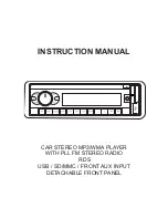
background image

– 1 –

MD-X60H

 CONTENTS

MD-X60H

SERVICE MANUAL

SHARP  CORPORATION

No.S6849MDX60H//

 • In the interests of user-safety the set should be restored to its original

condition and only parts identical to those specified should be used.

This document has been published to be used
for after sales service only.
The contents are subject to change without notice.

Page

SAFETY PRECATION FOR SURVICE MANUAL ..............................................................................................................  2
INPORTANT SERVICE NOTES (FOR U.K. ONLY) ........................................................................................................... 3
WIRING OF PRIMARILY SUPPLY LEADS  (FOR U.K. ONLY) .......................................................................................... 3
SPECIFICATIONS .............................................................................................................................................................  4
NAMES OF PARTS ...........................................................................................................................................................  5
OPERATION MANUAL ....................................................................................................................................................... 8
DISASSEMBLY ................................................................................................................................................................  10
REMOVING AND REINSTALLING THE MAIN PARTS ...................................................................................................  14
ADJUSTMENT .................................................................................................................................................................  17
EXPLANATION OF ERROR DISPLAY ............................................................................................................................. 27
EEPROM WRITING PROCEDURE .................................................................................................................................. 29
RDS OPERATION ............................................................................................................................................................ 31
NOTES ON SCHEMATIC DIAGRAM ..............................................................................................................................  35
TYPE OF TRANSISTOR AND LED .................................................................................................................................  35
WIRING DIAGRAM ..........................................................................................................................................................  36
BLOCK DIAGRAM ...........................................................................................................................................................  38
SCHEMATIC DIAGRAM / WIRING SIDE OF P.W.BOARD .............................................................................................  42
WAVEFORMS OF CD CIRCUIT ......................................................................................................................................  69
WAVEFORMS OF MD CIRCUIT .....................................................................................................................................  70
TROUBLESHOOTING (CD SECTION) ...........................................................................................................................  72
TROUBLESHOOTING (MD SECTION) ...........................................................................................................................  76
FUNCTION TABLE OF IC ................................................................................................................................................  81
REPLACEMENT PARTS LIST/EXPLODED VIEW/PACKING OF THE SET

Dolby noise reduction manufactured under license from Dolby
Laboratories Licensing Corporation.

"DOLBY" and the double-D symbol 

 are trademarks of Dolby

Laboratories Licensing Corporation.

Summary of Contents for MD-X60H

Page 1: ...OF PARTS 5 OPERATION MANUAL 8 DISASSEMBLY 10 REMOVING AND REINSTALLING THE MAIN PARTS 14 ADJUSTMENT 17 EXPLANATION OF ERROR DISPLAY 27 EEPROM WRITING PROCEDURE 29 RDS OPERATION 31 NOTES ON SCHEMATIC DIAGRAM 35 TYPE OF TRANSISTOR AND LED 35 WIRING DIAGRAM 36 BLOCK DIAGRAM 38 SCHEMATIC DIAGRAM WIRING SIDE OF P W BOARD 42 WAVEFORMS OF CD CIRCUIT 69 WAVEFORMS OF MD CIRCUIT 70 TROUBLESHOOTING CD SECTIO...

Page 2: ...attempt to interfere with the in terlock switch or make any other adjustment as this may result in exposure to hazardous radiation SAFTY ORECAUTION FOR SERVICE MANUAL WARNINGS CD THE AEL ACCESSIBLE EMISSION LEVEL OF THE LASER POWER OUTPUT IS LESS THAN CLASS 1 BUT THE LASER COMPONENT IS CAPABLE OF EMITTING RADIATION EXCEEDING THE LIMIT FOR CLASS 1 THEREFORE IT IS IMPORTANT THAT THE FOLLOWING PRECAU...

Page 3: ...ure 3 2 Magnetic Head Optical pickup Optical pickup Mechanism Chassis Spindle Motor Magnet Head Laser Beam Cartridge Holder NG The NG lamp lights and the buzzor sounds OK The GOOD lamp lights Judgment Unit Set current Cutoff current Set time Set name Withstanding Voltage Tester Test voltage Set value 4 240 VPEAK 3 000 VRMS 6 secs 4 mA Before returning the unit to the customer after completion of a...

Page 4: ...urable less than 0 001 W peak Tuner section Frequency range FM 87 5 108 MHz AM 522 1 620 kHz Sensitivity FM 2 5 µV 75 ohms unbalanced AM 650 µV m Cassette deck section Type Compact cassette tape Frequency response 50 14 000 Hz Normal tape 50 15 000 Hz CrO2 tape Motor DC motor with electronic governor 1 Signal noise ratio 50 dB Recording Playback Dolby NR off Dolby NR effect 10 dB at over 5 kHz Bia...

Page 5: ...PE 27 Edit Button MD TAPE MD TAPE 28 MD Name TOC Edit Button NAME TOC EDIT 29 TUNER Tuning Down Button 3 CD Track Down Review Button 3 MD Track Down Review Cursor Button 30 Jog Dial 31 TUNER Tuning Up Button 3 CD Track Up Cue Button 3 MD Track Up Cue Cursor Button 32 Enter Button ENTER 33 TAPE Dolby NR Button DOLBY NR 34 TAPE Reverse Mode Button REVERSE MODE 35 Edit Auxiliary 1 Analogue Input Sock...

Page 6: ...or AUTO MARK 17 MD Recording Mode Indicator MONO LP 18 Timer Play Timer Record Indicator 19 CD MD Programme Indicator PROGRAM 20 CD MD Random Play Indicator RANDOM 21 CD MD Repeat Indicator 22 RDS Indicator RDS 23 Traffic Announcement Indicator TA 24 Traffic Programme Indicator TP 25 EON Indicator EON 26 Programme Type Indicator PTY 27 Traffic Information Indicator TI 28 FM Stereo Mode Indicator S...

Page 7: ...5 Sound Synchro Record Button SOUND SYNCHRO 16 Auto Mark Button A MARK 17 Record Mode Button REC MODE CD control section 18 Track Up Cue Down Review Buttons 19 Play Pause Button 20 Stop Button 21 Play Buttons 1 2 3 22 Auxiliary Input Digital Analogue Select Button AUX 23 Display Button DISPLAY 24 Time Display Select Button TIME Tape control section 25 Fast Wind Buttons 26 Stop Button 27 Play Butto...

Page 8: ...the MD system the delimiter of the recording area on an MD is programmed in a TOC If partial erasing recording and editing are repeated several times TOC information will fill up even though the number of tracks has not reached the limit 255 tracks and further recording will be impossible If you use the all erase function this MD can be used from the beginning If there is any flaw on the MiniDisc ...

Page 9: ... Replace it with a regular disc that can be copied Can t EDIT A track cannot be edited Change the stop position of the track and then try editing it Can t REC Recording cannot be performed correctly due to vibra tion or shock in the unit Re record Can t T REC Timer recording is impossible or there is no available space on the MD Replace it with another disc CH ERROR There is something wrong with t...

Page 10: ...use PWB 1 Screw G1 x2 11 2 8 MD Holder 1 Screw H1 x4 11 2 3 9 MD Unit 1 Screw J1 x2 11 3 10 Front Panel 1 Socket K1 x1 11 4 2 Screw K2 x5 11 Power PWB 1 Screw L1 x5 11 4 12 Tape Mechanism 1 Screw M1 x4 11 5 13 Tray Switch PWB 1 Screw N1 x2 11 5 2 Socket N2 x1 14 Display PWB 1 Screw P1 x9 11 5 2 Flat Cable P2 x1 15 Switch A PWB 1 Screw Q1 x2 11 5 16 Switch B PWB 1 Knob R1 x1 11 5 2 Nut R2 x1 3 Scre...

Page 11: ...nel MD Unit MD Holder Fuse PWB Power Amp PWB Fan Motor J1 x1 ø3 x10mm J1 x1 ø1 7 x3mm H1 x1 ø3 x10mm Front Panel MD Holder MD Unit K1 x1 L1 x1 ø3 x8mm K2 x2 ø3 x10mm K2 x3 ø3 x8mm L1 x4 ø4 x8mm Front Panel Power PWB Pull Pull R1 x1 R2 x1 P2 x1 N2 x1 S1 x1 N1 x2 ø3 x10mm P1 x9 ø3 x10mm R3 x5 ø3 x10mm R4 x1 ø3 x8mm S2 x1 ø3 x10mm T1 x1 ø3 x10mm Lug Wire Q1 x2 ø3 x10mm M1 x4 ø3 x10mm U1 x1 ø3 x10mm F...

Page 12: ...e uppermost position CD Mechanism Pawl Push Spring V4 x3 W1 x 1 ø2 x 4mm W1 x 1 ø2 x 4mm W1 x 1 ø3 x 10mm W1 x 1 ø3 x 10mm W1 x 1 ø2 x 4mm W1 x 1 ø2 x 4mm W1 x 1 ø3 x 10mm W1 x 1 ø3 x 10mm MD Unit shield Case Upper shield Case Below MD Holder MD Holder Bracket X3 x1 X2 x1 X2 x3 X2 x1 X1 x4 ø1 7 x 3mm MD Main PWB Pull W4 x1 Chassis Optical pickup Flexible PWB Note 1 Note 1 After removing the flexib...

Page 13: ...chanism A1 x1 A2 x1 Woofer Front Panel Super Tweeter Tweeter Net A3 x2 ø3x10mm A3 x3 ø3x8mm A3 x1 ø3x6mm A3 x4 ø4x16mm Woofer Super Tweeter Tweeter Front Panel 1 Speaker 1 Net A1 x1 13 2 2 Front Panel A2 x1 3 Screw A3 x10 13 3 STEP REMOVAL PROCEDURE FIGURE SPEAKER SPEAKER ...

Page 14: ...to the rear side 2 Apply 5V to the red line side of blue connector of loading motor push the rack gear in the arrow direction to move the cam plate lever until tick is heard 3 Remove the screw B1 x1 pc and the spring B2 x1 pc fitted to the holder arm and shift the cartridge holder to the left side to remove it How to remove the mechanism switch PWB See Fig 14 3 1 Removethescrews C1 x2pcs andremove...

Page 15: ...Caution Be careful so that the gear is not damaged The damaged gear emits noise during searching How to remove the sled motor loading motor See Fig 15 1 1 Remove the screws D1 x 4 pcs and remove the sled motor loading motor Caution Be careful so that the gear is not damaged The damaged gear emits noise during searching Figure 15 1 Spindle Motor Turntable Gear E1 x3 Ø1 7x2 5mm Optical Pickup F1 x3 ...

Page 16: ...ray See Fig 16 4 1 Remove the cabinet and front panel 2 Disassemble as shown in the figure so that the CD disc of CD changer can be taken out 3 Remove the CD disc from the tray as shown in the figure How to remove the CD disc When CD is in playback state See Fig 16 3 1 Remove the cabinet and front panel 2 Disassemble as shown in the figure so that the CD disc of CD changer becomes visible 3 Remove...

Page 17: ...ion fH 1 620 kHz Tracking fL T302 990 kHz Set the output of speaker terminal to maximum AM signal oscillator Frequency 400 Hz 30 AM modulation FM mute level adjustment Frequency Adjusting object Adjusting method 98 MHz 30 dB VR351 Input SO301 Output Speaker Terminal FM signal oscillator Frequency 400 Hz 22 5 kHz Adjusting object Preset No Frequency Figure 17 2 FM Mute Level Table 17 Initial settin...

Page 18: ...Point Specified Value Instrument Connection Raise the cassette holder cover and remove it and then adjust the azimuth 102 7kHz TP101 IC102 pin 3 Checking the bias oscillation Frequency Adjusting Point Specified Value Instrument Connection Adjusting the deck circuit Adjusting the mechanism VOLUME MAX FUNCTION TAPE TAPE NORMAL DOLBY NR OFF REVERSE MODE NORMAL BEAT SW A Position of each swich or cont...

Page 19: ... the pickup with the or button Cancel method POWER OFF Initialization is not performed CD SECTION Since this CD system incorporates the following automatic adjusting function when the pickup is replaced it is not necessary to the readjust it Since this CD unit does not need adjustment the combination of PWB and laser pickup unit is not restricted Automatic adjustment items 1 Focus Offset Fig 19 1 ...

Page 20: ...f mechanism pickup and PWB was changed set the TEST mode to perform the AUTO preliminary adjustment and AUTO adjustment write the adjustment data in EEPROM When EEPROM was replaced set the TEST mode write the EEPROM set data p29 p30 and then perform the preliminary adjustment and AUTO adjustment write adjustment data in EEPROM Figure 20 Conection of Extention Cable 5Pin extension flat cable QCNWK0...

Page 21: ...is performed The adjustment value is output with the aid of system controller interface Continuous playback is performed Error rate indication jump test RESULT sub mode RESULT mode final adjustment MANUAL pre adjustment mode MANUAL adjustment mode 4 EEPROM setting mode Various coefficients of digital servo are changed manually 5 TEST PLAY mode Continuous playback from the specified address is perf...

Page 22: ...4 Press once the CD STOP button Playback power output state p p w _ _ _ _ _ _ _ Step 5 Press the CD MD EDIT button TEMP setting of EEPROM setting Refer to TEMP setting of EEPROM Step 6 Press the TRACK EDIT button CONTROL setting of EEPROM setting Refer to CONTROL setting of EEPROM Step No Setting Method Remarks Display 2 AUTO pre adjustment mode Low reflection disc only Step No Setting Method Disp...

Page 23: ...CD PLAY button S P G _ m i d _ Step 8 Press once the CD PLAY button S P G _ o u t _ Step 9 Press once the CD PLAY button S P 1 _ _ _ _ _ Step 10 Press once the CD PLAY button S P 2 _ _ _ _ _ Step 11 Press once the CD PLAY button S P 3 _ _ _ _ _ Step 12 Press once the CD PLAY button S P 4 _ _ _ _ _ Step 13 Press once the CD PLAY button S P 5 _ _ _ _ _ Step 14 Press once the CD PLAY button S P D L I...

Page 24: ... T R L 1_ Step 6 Press once the CD PLAY button C O N T R L 2_ Step 7 Press once the CD PLAY button S P K L E V m_ Step 8 Press once the CD PLAY button A D J T T M_ _ Step 9 Press once the CD PLAY button H D E Q A D_ _ Step 10 Press once the CD PLAY button L D E Q A D_ _ Step 11 Press once the CD PLAY button G D E Q A D_ _ Step 12 Press once the CD PLAY button H D E Q B C_ _ Step 13 Press once the ...

Page 25: ...start continuous play a p w return it to L Continuous recording Step 5 Press once the MD STOP button TEST REC menu T E S T _ R E C _ _ Step No Setting Method Remarks Display If the MD STOP button is pressed while the TEST PLAY menu is displayed TEST mode STOP state is set If the MD PLAY button is pressed while the TEST REC menu is displayed continuous record is started from the current pickup posi...

Page 26: ... I N N E R _ _ Step 3 Press once the MD PLAY button INNER switch position measurement s c SUBQ address and C1 error are also indicated Step 4 Press once the MD STOP button INNER menu _ _ I N N E R _ _ Step No Setting Method Remarks Display Figure 26 2 Figure 26 4 Loosen the two screws A Lead In Switch Mechanism Switch PWB 1 2 3 1 2 3 adjusting hole Spindle motor Check the Lissajou s waveform shift...

Page 27: ...ata resulting in record failure TOC was read but data was not correct TOC could not be rad Trouble occurred during rewriting of UTOC resulting in UTOC rewriting failure After the disc was loaded focusing failure occurred EXPLANATION OF ERROR DISPLAY Error display Errors Corrective action Can t REC Can t COPY Din UNLOCK TOC FULL UTOC ERR R UTOC ERR A UTOC ERR L0 4 NOT AUDIO DISC DISC FULL PLAYBACK ...

Page 28: ...t fingerprint and black spot Check for disc disalignment and run out Check that the record head contact is normal Check that there is no broken wire between PWB and the recording head Perform adjustment Once reset and redo If error occurs persistently replace EEPROM EXPLANATION OF MECHANISM ERROR Error display Errors M E C H A _ E R R 1 _ Ejection failure M E C H A _ E R R 2 _ Head up failure M E ...

Page 29: ...E T 3 Press the MD PLAY button 7 times F O C U S 4 Press the CD PLAY button 4 times T e m p 5 Press once the MD PLAY button T E M P Measured temperature Temperature setting 6 Set temperature to the value determined above using JOG DIAL UP or JOG DIAL DOWN 7 Press the MD STOP button T e m p 8 Write in EEPROM by pressing ENTER button Ambient temperature correction 21 0 C 22 3 C 0 1 H 22 3 C 26 3 C 0...

Page 30: ... T F 2 _ _ _ _ _ T R B L V o _ _ T R B L V t _ _ T R K L V o _ _ T D P W o _ _ _ S L C T o _ _ _ S L C T t _ _ _ S L C T m _ _ _ C O T L V p _ _ C O T L V r _ _ T D P W t _ _ _ T R K L V t _ _ S P G _ _ _ _ _ S L G _ _ _ _ _ T E M P_ _ C O N T R L 1 _ C O N T R L 2 _ S L 2 _ _ _ _ _ S L D L E V _ _ S L K L V k _ _ S L K L V t _ _ S L K L V m _ _ S P 1 _ _ _ _ _ S P 2 _ _ _ _ _ S P 3 _ _ _ _ _ S P ...

Page 31: ...rmation Provided by RDS With the MD X60H you can display two types of RDS service To show them in the display press the DISPLAY button Each time you press the DISPLAY button the display will change to show the following information PS Programme Service Station names commonly known will be diaplayed PS appears if no signal is being sent PTY Progamme Type Programme type will be diplayed PTY appears ...

Page 32: ...th same format ASPM operation untill 108 MHz After reached 108 MHz displayed the TTL quantity of memorized stations And return to the previous receiving freq automatically Displayed the TTL quantity of memo rized stations by ASPM operation on this time And return to the previous receiving freq automatically Yes No Yes Yes Yes Yes No No No No No No Effect Pass No effect Pass No effect Pass No effec...

Page 33: ...ind light up or go out individually TA ind doesn t light up on current model CD C75H due to none EON TI 3 Added 3 indicators in FL due to adding EON feature EON Lights up only during receiving EON data 14A TI During EON TI stand by Light up During receiving ON station blink PTY During EON PTY stanb by Light up During receiving ON station blink 4 No adjust type None adjusting circuit 5 Added EON bu...

Page 34: ...station is NO RDS NO signal TA OFF or different PTY items The receiver switch back ON TN displaying NO READY 13 During receive ON station when ON station become to be NO RDS NO signal TA ON to OFF or different PTY item The receiver switch back ON TN 14 EON TI PTY Switch TN ON in case of 2 more stations exist comparing field strength and switch to the strongest station if these signals are same str...

Page 35: ...the resistor without any symbol is ohm type resistor Besides the one with Fusible is a fuse type Capacitor To indicate the unit of capacitor a symbol P is used this symbol P means micro micro farad and the unit of the capacitor without such a symbol is microfarad As to electrolytic capacitor the expression capacitance withstand voltage is used CH TH RH UJ Temperature compensation ML Mylar type P P...

Page 36: ... RD FWM2 CNS103 CNS102 13 TAPE MECHANISM PWB F TAPE MOTOR MM1 217 2 B RECORF PLAY BACK ERACE HEAD 217 1 BK GY WH CNS101B CNS101A WH 1 7 6 1 6 1 FLEXIBLE PWB TAPE HEAD PWB G WH WH FLEXIBLE PWB FLEXIBLE PWB SW1 SW2 SW3 SW4 SW5 1 7 JK401 SW101 CNS706 B 1 2 1 2 RD WH DECK SWITCH PWB B6 CNP703 1 2 CD EJECT SWITCH PWB B7 MD INPUT LEVEL PWB B4 VR630 CNS630 1 1 1 3 8 11 CNS6011 6 OPERATION PWB B2 TUNER PW...

Page 37: ... 1 7 1 8 1 2 1 2 WH BK 1 3 12 1 11 14 1 9 1 2 1 6 1 5 1 4 CNP102 CNP930 CNP2 CNP3 UNA901 DIGI IN CNP1 BK WH CNP11 CNP990 CNP980 CNS970 CNS970A CNP960 CNP550 SW901 1 8 CNP940 CNP925 CNP103 1 8 1 13 CNP401 GY JK401 CNP950 SW951 CNP910 1 15 1 CNP920 1 23 2 24 6 1 CNS802B 1 12 1 13 CNS801B T801 POWER TRANSFOMER CNP801 1 7 1 3 CNS850 CNS801A 1 13 1 12 CNS802A K802 K801 CNP261 1 2 CNP850 CNS851 1 7 TO M...

Page 38: ...A GND L IN L OUT LOAD IN RESET MD ST DSCK SERCH 1 2 24 23 22 21 20 19 18 17 16 15 14 4 5 6 7 8 9 13 10 11 12 3 D GND D GND D GND D GND DSTB MDDATA KDATA 4M DRAM ENDEC ATRAC IC1201 OSCILLATOR XL1201 33 8688MHz SW1956 SW1955 SW1954 SW1953 SW1952 Q1251 Q1254 MD RECORDING HEAD M901 SPINDLE MOTOR M902 SLED MOTOR M903 LOADING REC PLAY LEAD IN A BSIGNAL E FSIGNAL RF1 RF4SIGNAL HEAD DRIVE SIGNAL IC1251 RF...

Page 39: ...ONTROL CE SL SL DRF CD D OUT 7 3 5V 62 64 77 47 27 79 56 72 68 63 11 13 15 32 40 43 44 53 52 51 54 31 30 29 23 27 16 15 54 78 Q1 5V 5V VOLTAGE REGULATOR Q81 7 3V B2 IC91 TA7291S TRAY MOTOR DRIVER XOUT EFMIN 10 EFMO CLV JP TGL TOFF TES HLF V P JP 19 20 23 24 28 29 76 75 51 50 40 39 8 4 2 VVDD VDD LVDD RVDD XVDD MAIN SECTION 6 1 9 5 IC92 TA7291S MAIN CAM MOTOR DRIVER 7 3 M M MOB1 MAIN CAM MOTOR TO µ...

Page 40: ... T306 T302 DO CE CL DI FM FRONT END FE301 Q360 MUTING MPX VCO CUT LOW PASS FILTER R L Q353 Q354 MPX IN FM AM OUT IF IN SD FM MONO ST MONO ST AM RF IN AFC IN OUT VR351 FM MUTE LEVEL AM OSC IN OUT VCC FM IF IN FM IF AMP Q301 AMP QT21 FM IF CF301 FM IF FM OSC STEREO AM IN FM IN FMOSC T351 AM IF GND OSC FM AM RF AM ANT FM 75ohms AM OSC CF352 L354 CNP301 SO301 ANTENNA TERMINAL AM LOOP ANTENNA Q371 Q361...

Page 41: ...OG701 VOLUME Q501 Q502 B4 B5 REMOTE SENSOR 1 2 3 B5 B5 B5 SW951 RESET 47 49 12 10 L R L L R L R 30 7 L R 29 8 14 3 16 1 L R L R L R 22 23 R L L R R L R L R L R L R L R L R 71 80 93 2 1 99 57 92 91 85 NAME IN APSS IN REC MUTE REC MUTE CONTROL CrO 2 SWITCHING DORBY RWC PB DORBY ON OFF PB MUTE PLAY MUTE CONTROL SWITCHING BIAS COTROL BIAS OSC SWITCHING SWITCHING REC CONT REC BIAS MOTOR SOL RUN PLSE BU...

Page 42: ... R133 1K C148 10 16 C102 560P C142 560P C105 0 033 R107 3 9K C101 560P C130 33 16 R101 1K C125 10 16 R124 100K C113 1 50 R136 10 R 5 Q10 2SB 2 R152 560 6 5 4 3 1 2 6 5 4 3 1 2 7 6 1 2 3 4 5 7 6 1 2 3 4 1 2 3 4 5 6 7 8 9 11 10 12 13 14 15 16 17 18 26 27 25 24 23 22 21 20 19 35 36 34 33 32 31 30 29 28 5 1 2 3 4 5 6 7 8 9 B B RECORD PLAYBACK HEAD ERASE HEAD R CH L CH EH 2 3 1 2 1 3 3 2 1 3 2 1 3 2 1 ...

Page 43: ...C167 10 16 R173 18K C169 4 7 50 R159 2 2K C155 220P C173 10 16 C172 1 50 1 2 3 4 5 6 7 8 9 1 2 3 4 5 6 7 8 9 10 11 12 13 10 11 12 13 9 8 7 6 5 4 3 2 2 1 1 11 10 11 10 9 8 7 6 5 4 3 2 2 1 1 1 2 3 4 5 6 7 16 15 14 13 12 11 10 8 9 3 2 1 SW SW BUF AMP SIDE CHAIN SIDE CHAIN REC IN PB IN PB IN REC IN PB OUT NR ON OFF DET MECHA GND CR02_SW REC CONT SOL A D 5V MOTOR RUN_PLSE MAIN_SW R P CR02 APSS IN CASST...

Page 44: ...D LOAD SYN RLY_OUT POWER DSLK K DATA MD DATA CQCK COIN SQOUT AVREF1 JOG A VSM DATA CLK LCK1 WRQ TRY SW2 TRY SW3 SUB CLK OUT SUB CLK IN AVSS PROTECT AVDD AVREF0 SPE_ANA L SPE_ANA R VSS DATA CLK VDD OE SW2 SW1 SW3 DRF RES SW4 SW5 PLAY 1T SW12 LCK1 MAIN CLK OUT JOG B LCK2 INITIAL AREA 1 SPE_ANA A NAME SEL SW10 SW11 DATA SEL NEXT NAME IN TRY SW4 TEST VPP MAIN CLK IN RDS RWC PLAY N SKIP 10 SKIP 1 DUBB ...

Page 45: ...cc MD_A_GND MD_A_GND VLOAD EEP DO EEP DI EEP SK EEP CS MIC IN SD MOTOR SIDE A SW CASSETTE SW CrO2 SW SIDE B SW RUN PULSE APSS OE VDD CS SK DI DO SW9 SW8 SW7 SW5 SW11 SW10 SW12 P_DOWN TAPE DSTB MDDATA AD_GND D_GND D_GND LOAD_SW D_ B D_GND MD D_GND MD D_GND MD D_GND MD RESET MD_ST DSCK SEARCH DSTB MDDATA KDATA DSCK KDATA SQOUT COIN CQCK RWC RES_CD WRQ L_MUTE CCB_CE CCB_CL CCB_DO PU_IN RESET SEARCH M...

Page 46: ...50 C578 47P CH R568 1K R567 1K R565 2 7K C571 22 50 R566 2 7K C572 22 50 IC552 NJM4565M BUFFER AMP C573 82P CH R569 10K 63 64 59 58 1 2 3 4 5 6 7 8 9 10 11 12 13 14 15 16 17 18 19 20 21 22 23 24 25 26 27 28 29 30 31 32 33 34 35 36 37 38 39 40 41 24 43 44 45 46 47 48 49 50 51 52 53 54 55 56 57 58 59 60 61 62 63 64 55 51 50 8 4 2 3 5 6 7 1 68 67 66 56 53 54 52 65 61 62 60 57 TP402 TP401 REC RCH REC ...

Page 47: ...D421 1SS133 D422 1SS133 L422 2 2µH L421 2 2µH L423 2 2µH R401 1K 1 2 3 4 5 6 7 8 1 2 3 4 5 6 7 8 3 2 1 1 3 2 1 2 3 4 5 6 1 2 3 4 5 6 1 2 3 4 5 6 1 2 3 4 5 6 7 8 9 10 11 4 8 11 1 7 14 12 10 13 2 9 6 3 5 2 33 34 35 36 37 38 39 40 41 24 43 44 45 46 47 48 9 23 22 20 21 CNS550 CNS401 CNS630 REC RCH REC LCH _IN L _IN R B MD INPUT LEVEL PWB B4 1 4 2 5 3 AUX LIN_VOL OUT AUX RIN_VOL OUT AUX GND AUX LIN_VOL...

Page 48: ...5 18 C105 1 5 8 9 10 15 16 1 5 10 15 20 25 30 31 35 40 45 50 51 55 60 65 70 75 80 81 85 90 95 B C E B C E 100 B A C905 R501 R503 R50 R504 R R9 R962 C964 R1057 R1058 R954 R953 C951 C952 R941 C941 C942 R923 R924 R925 R926 R927 R929 R930 R931 R932 R933 R1024 R1025 R1026 R1027 R1029 R1030 R1031 R1032 Q951 RA243 RA242 RA241 R912 R913 C915 C914 R1056 C918 C998 R1055 Q115 R187 R186 R195 R194 R906 R907 R9...

Page 49: ... 18 10 10 9 9 1 1 5 5 15 15 1 5 10 15 20 24 25 30 35 40 41 45 50 55 60 64 65 70 75 80 6 5 4 3 2 1 1 5 10 15 18 19 20 25 30 35 36 40 45 50 51 55 60 5 BK WH 1 4 5 8 1 5 7 8 10 14 X902 TP XL1 C54 C56 C22 C55 C58 C57 R46 R47 R60 C62 C61 R36 C33 R61 C60B R58 C42 R57 R38 R56 C31 R37 R34 R35 R32 C32 R33 C30 C46 C51 R70 CA13 RA234 RA233 C86 R89 C84 R91 R90 C87 C96 R97 C94 C97 R96 R98 C929 C930 C931 C932 C...

Page 50: ...10 9 8 23 24 25 26 27 28 29 30 31 32 33 34 35 36 7 6 5 4 3 2 1 1 2 3 4 5 6 7 8 9 10 11 12 13 14 15 16 33 34 35 36 37 38 39 40 41 42 43 44 45 46 47 48 SP PU_IN SL_ SL_ VREF GND MON VR1A TR TR FO FO VCC 1 2 VCC E A B F C LD ACTUATOR LTOH41M1 C3A C F B A E VREF IN RVEF OUT NC GAIN1 VCTL1 VM1 VM1 GND GND GND GND VM2 VM2 VCTIL2 GAIN2 NC VCC REG5V STANDBY SS GND STANDBY GAIN4 VCTL4 VM4 VM4 GND GND GND G...

Page 51: ...AY MOTOR MT MT MAIN PWB A 4 4 FSEQ RES CD_9V CD_GND MO_H L C_MO_FOR C_MO_REV T_MO_FOR T_MO_REV WRQ RWC SQOUT DRF SL CQCK COIN CD_7V CD_D_OUT DIG_GND RVSS LVSS DOUT EFLG SFSY PW SBCK TEST1 EFMO EFMIN TEST2 MUTER LVDD MUTEL X TAL GENERATOR 4M 16M RES CQCK COIN SQOUT RWC FSX SUB CODE SBSY XVSS XIN XOUT XVDD RVDD TEST4 DAC 8fs OVER SAMPLING DIGITAL FILTER DIGITAL OUT ERROR COERECT FLAG CONTROL VCO CLO...

Page 52: ...01 RD BK R1901 R1902 R1903 R1904 1 2 BK BK CN1901 SW1955 RECORD SW1953 LEAD IN MAGNET HEAD 40 SW1954 PLAY SW1956 LOADING SW1952 DERECT LOADING MOTOR M903 1 2 FLEXIBLE PWB RD BK 1 2 RD BK 1 2 BR COLOR TABLE RD R OR YL GR BL VL GY WH W BK PK BROWN RED ORANGE YELLOW GREEN BLUE VIOLET GRAY WHITE BLACK PINK MD MECHANISM SWITCH PWB E ...

Page 53: ...WITCH PWB I M702 SW702A SPINDLE MOTOR SLED MOTOR PICKUP IN M701 CNP3A 1 2 3 4 5 6 CD MOTOR PWB H 7 6 5 4 3 2 1 7 8 6 5 4 3 2 1 PICK UP UNIT YL BIMO1 TRAY MOTOR MAIN CAM MOTOR MOB2 MOB1 BR YL OR RD BR 1 2 3 4 SWB101 CAM1 SWB102 CAM2 SWB103 BIMO3 CAM3 SWB104 CAM4 BL BR 6 1 2 3 4 5 SOLENOID SOL 1 TAPE MECHANISM PWB F TAPE MOTOR MM1 217 2 B RECORF PLAY BACK ERACE HEAD 217 1 1 2 3 4 5 6 FLEXIBLE PWB TA...

Page 54: ...SDATA P1 P0 VCC1 XOUT XIN VSS SEG35 SEG34 SEG33 SEG32 SEG31 SEG30 SEG29 SEG28 SEG27 VP DIG4 CS SIN SOUT SCLK VEE VEE DIG0 DIG1 DIG2 DIG3 VDD XOUT VSS XIN RESET AN5 AN4 AN3 AN2 AN1 AN0 VDD SEG9 SEG8 SEG7 SEG6 SEG5 SEG4 SEG3 SEG2 SEG1 SEG0 DIG5 DIG6 DIG7 DIG8 SEG16 SEG15 SEG14 SEG13 SEG12 SEG11 SEG10 FILMNT2 FILMNT2 FILMNT2 FILMNT2 FILMNT2 FILMNT2 GP5 GP4 GP3 D H GP14 GP13 GP12 GP11 GP10 GP9 GP8 GP7...

Page 55: ...71 BU2092F INPUT OUTPUT EXPANDER C755 1 50 C753 390P CH C752 150P CH R709 1K LED779 LED774 KL052UL R728 820 R729 820 R726 820 LED773 KL052UL LED772 KL052UL R725 820 R727 820 R720 680 LED780 R750 820 LED776 LED771 KL052UL LED775 KL052UL SW737 R736 6 8K SW736 R730 680 LED782 1 2 3 1 2 1 2 3 2 1 1 2 3 4 2 1 2 1 1 2 1 2 3 1 2 3 4 5 6 7 8 9 10 11 12 13 14 15 16 17 18 POLE POSITION K5052UL GREEN KL052UL...

Page 56: ...771 LED772 LED773 SW732 NAME TOC EDIT LED778 LED777 LED780 LED779 LED782 LED781 SW744 UP SW741 DOWN SW751 POLE POSITION SW747 CD TAPE EDIT SW748 MD TAPE EDIT LED774 LED775 LED776 JOG701 VR630 INPUT LEVEL VOLUME MAX MIN CNS630 1 2 3 4 5 6 7 8 9 10 11 L631 CNS601 1 2 3 4 5 6 JK620 HEADPHONES R626 R625 L601 CNS620 1 2 3 4 5 6 C625 C626 R718 C706 R735 R734 R733 R707 R719 C708 R709 C753 R708 C751 C752 ...

Page 57: ...1 5 10 11 12 15 20 22 23 25 30 33 34 35 40 44 4 5 8 35 40 45 50 55 60 64 C730 L733 L731 L732 C746 C744 C745 CNS704 1 2 3 SW706 MD STOP SW705 MD PLAY SW716 DISC3 EJECT SW736 DOLBY NR SW737 REVERSE MODE SW717 DISC2 EJECT SW718 DISC1 EJECT CNP703 1 2 DISPLAY PWB B1 CD EJECT SWITCH PWB B7 CNS706 B 1 2 DECK SWITCH PWB B6 R717 R716 R736 R764 R724 C783 C784 C785 C786 C787 C788 C789 R712 R715 R714 R713 R7...

Page 58: ...012 C852 0 022 R852 220 R853 1K C853 0 022 C833 100 16 C205 470P C868 0 022 C882 0 022 ZD821 MTZJ8 2B C830 0 022 R830 1K RP880 C885 0 022 C884 220 16 Q881 KRC102 M C241 47 25 ZD241 MTZJ11C C242 0 022 R243 820 3W Q811 2SD2012 C815 100 10 C818 0 022 C816 100 10 R811 100 C817 0 022 ZD810 MTZJ5 6C RP811 POSISTOR POSISTOR POSISTOR POSISTOR POSISTOR POSISTOR POSISTOR R862 680 Q863 KRA102 M Q862 KRC1 C82...

Page 59: ... ZD802 MTZJ360D R802 1K C811 220 63 D817 1N4004S D818 1N4004S Q801 2SB1565 F D819 1N4004S FR801 2 2 T801 POWER TRANSFORMER D804 1N4004S D803 1N4004S D805 1N4004S D802 1N4004S ZD803 MTZJ10C Q805 2SB1565 F CNP850 CNS850 1 13C OSISTOR Q863 KRA102 M Q862 KRC102 M R863 47K 6 5 4 3 2 1 6 5 4 3 2 1 2 3 1 6 5 4 1 2 M 1 2 13 12 11 10 9 8 7 6 5 4 3 2 1 3 2 1 7 6 5 4 3 2 1 11 13 12 12 12 11 11 10 10 10 9 9 9...

Page 60: ...02 T5A L 125V CNS802B 1 4 7 8 11 12 1 4 7 8 13 12 CNS801B AC POWER CORD AC 230V 50Hz 257 CORE 261 T801 POWER TRANSFORMER C804 C810 R802 ZD802 C812 FR801 R805 Q805 B C E E C B Q801 D805 D804 C803 D803 D802 D815 C805 D812 D813 C806 D814 C811 R803 POWER PWB C2 C813 ZD803 D819 D818 D817 D816 C808 C891 C809 CNP801 1 7 6 5 4 3 2 1 2 3 CNS850 C801 C802 CNS801A T F801 1 4 7 8 12 13 1 4 7 8 11 12 CNS802A K...

Page 61: ...241 C203 R203 C221 R201 D203 R246 R245 R272 R240 R228 R233 R236 R235 R234 C220 R261 1 2 3 4 5 6 7 8 9 10 11 12 13 14 15 R263 FR201 FR202 R244 C215 C223 C238 C205 C206 R212 C237 Q253 R247 R211 C262 C209 C243 RP870 R879 R880 ZD882 ZD881 C880 R881 C210 C261 R205 R206 J82 C888 CNP850 1 2 3 4 5 6 7 Q881 C882 C884 Q863 R863 R861 C885 C861 C868 C860 Q862 IC201 C207 R209 R210 C208 Q861 Q880 C867 ZD861 R25...

Page 62: ...C1102 1 TP1138 TP1139 TP1140 TP1141 Q1401 RN2404 C1407 Q1402 RNC1404 R1471 10K R1425 2 7K R1427 4 7K IC1251 74ACT02F HEAD DRIVER L1601 1µH CN1604 CN1603 CN1602 TP1128 TP1127 TP1126 TP1120 TP1104 TP1103 TP1102 TP1101 TP1109 TP1112 TP1113 TP1108 TP1114 TP1115 TP1116 TP1118 TP1119 TP1105 C1145 0 033 R1166 1 2K L1101 10µH C1121 1 TP1106 TP1107 TP1111 R1420 1K R1408 100K C1401 0 047 C1403 680P R1415 1K...

Page 63: ... R1474 1K C1405 0 1 IC1402 S29294A R1414 10K R1416 10K R1473 100K TP1455 TP1456 TP1457 R1476 1K C1406 1 TP1217 TP1218 TP1216 C1207 1 C1210 1 R1456 1K R1202 1M C1204 12P CH XL1201 C0001AW R1201 150 C1205 12P CH R1418 47K C1407 0 022 Q1402 RNC1404 R1471 10K R1969 56 C1954 15P CH C1952 0 01 R1962 220K C1955 0 047 C1958 0 047 R1965 10K R1963 1 5K C1956 47 6 3 C1953 0 47 IC1907 TC9246F CLOCK GENERATOR ...

Page 64: ...1827 R1466 R1464 R1462 R1460 R1458 R1454 R1452 R1456 C1904 Q1451 Q1821 Q1404 Q1403 C1927 J1921 IC1251 Q1254 Q1253 C1255 C1254 R1223 R1967 R1969 R1968 R1964 IC1916 IC1202 C1206 IC1906 IC1907 C1964 C1958 R1965 C1951 R1409 IC1990 C1954 R1963 R1962 C1955 C1990 D1990 C1953 C1992 R1961 C1952 CN1603 L1601 R1668 R1669 R1617 Q1601 R1609 R1612 R1611 C1604 R1610 R1614 R1613 C1610 XL1201 C1207 RC120 C1203 R12...

Page 65: ... TP1616 TP1609 C1657 R1664 TP1608 C1602 C1656 R1662 TP1610 TP1611 CN1604 C1605 R1660 C1655 C1609 C1654 R1658 TP1103 TP1104 TP1129 TP1218 C1631 IC1601 TP1216 TP1116 TP1141 TP1150 TP1122 TP1108 TP1112 L1101 C1121 R1665 R1663 R1661 R1659 TP1107 TP1105 TP1109 R1653 R1651 TP1220 TP1275 R1281 R1254 C1601 C1653 R1656 C1652 R1654 R1657 R1655 TP1106 C1661 TP1612 TP1111 TP1204 C1650 R1650 R1652 C1651 R1150 ...

Page 66: ...1K R372 1K R374 1K R371 1K C350 0 022 C352 10 16 C344 33P CH C351 0 022 R351 5 6K C399 C353 0 022 C354 0 022 R393 1K C364 10 16 C366 0 001 C365 0 022 C363 0 022 C343 33P CH VR351 10K B D301 1SS133 CNP301 R349 33 R344 470 R345 4 7K R301 330 C346 0 022 C345 0 022 C321 100 16 R379 2 2K C382 15P C381 12P X352 4 5MHz C385 0 01 R377 47K L351 100µH 10 R358 8 2K C342 0 022 R3 27 IC303 LA1832 CF351 C361 0 ...

Page 67: ...0 022 C353 0 022 C354 0 022 R393 1K C358 1 50 ZDT351 MTZJ5 1B RT49 390 RT48 390 CT43 10 16 RT21 100K RT26 1K RT28 1K RT30 1K LT22 2 2µH RT37 220K RT36 220K C364 10 16 C366 0 001 C365 0 022 R356 1K C369 27P C373 0 018 C374 0 018 R357 470K R364 100K C385 0 01 R377 47K L351 100µH R363 100K R366 10K R368 33K R365 10K C375 3 3 50 R367 1K Q353 KTC3199 GR Q354 KTC3199 GR X351 10 7MHz C368 1 50 R353 270 I...

Page 68: ...D301 2 L342 R349 C321 D301 D302 SO301 ANTENNA TERMINAL X352 1 5 10 11 12 15 22 20 VR351 C394 C380 L351 C393 R336 R382 D351 D352 R377 C375 C370 T351 NC Q361 C391 ZD352 R395 L352 R391 R392 C396 ZD351 Q371 IC302 T302 B C E B C E Q354 Q353 X351 IC303 VD301 1 FE301 1 2 3 4 5 6 7 8 Q360 CNP303 R370 1 2 3 4 5 6 7 8 9 10 11 12 13 TUNER PWB B3 3 2 1 B C E E C B B C E 1 2 3 3 3 2 1 2 1 R366 R362 R365 R361 R...

Page 69: ...P CUE 50ms 10 0 V JP 50ms 0 50 V JP 50ms 1 00 V TE 6 7 8 9 0 5ms 10 0 V JP 0 5ms 10 0 V JP 0 5ms 0 50 V JP 0 5ms 1 00 V TE 6 7 8 9 REVIEW 50ms 10 0 V JP 50ms 10 0 V JP 50ms 0 50 V JP 50ms 1 00 V TE 6 7 8 9 PLAY 20ms 1 00 V SPO NORMAL DISC TN0 01 20ms 2 00 V CLV 10 11 PLAY TCD 712 140mm TN0 01 50ms 1 00 V SPO 50ms 2 00 V CLV 10 11 PLAY TCD 712 5s 100mV SLD 1 12 0 5s 100mV SLD 1 12 0 5ms 10 0 V JP 0...

Page 70: ...1137 TEOUT TP1144 TOTAL TP1143 TCRSO 8 13 1 14 Stopped 1 2 4 MODISC NORMAL PLAY CH1 500mV 500µs div DC P 10 CH2 500mV DC P 10 CH4 2V DC P 10 10 0 100 90 TP1104 T TP1106 T 15 16 Filter SMOOTH ON Stopped NORM 5k S s TP1136 RESET Standby PLAY Standby FEOUT CH1 1 V 200ms div DC 10 1 CH2 500mV DC 10 1 CH3 5 V DC 10 1 CH4 5 V DC 10 1 V1 1 2 000V 1 V2 1 960 0mV V 1 1 040V MAIN 10K MIN AUTO EDGE CH1 0 000...

Page 71: ...H1 2V 5µs div DC P 10 CH2 2V DC P 10 CH3 2V DC P 10 10 0 100 90 DASDA ADBCK ADWS PLAY RECORDBLE MD MO DISC 20 21 22 Stopped 1 2 CH1 2V 5µs div DC P 10 CH2 2V DC P 10 10 0 100 90 SYSCLK DABCK PLAY 23 24 Stopped 1 2 CH1 2V 1µs div DC P 10 CH2 2V DC P 10 10 0 100 90 SYSCLK DABCK 23 24 Stopped 1 CH1 1V 500µs div DC P 10 10 0 100 90 VOUTL VOUTR PLAYBACK 1kHz 0dB V 6 48V 2 80V 3 68V 6 48V 25 Filter SMOO...

Page 72: ...04 and tray switch SWB105 to SWB108 Yes Yes Check the connection between IC901 and SW No ICheck whether output of pins 3 and 7 of main cam motor driver IC92 is normal Check the connection from IC2 of pins 24 and 25 to IC92 No Yes Check whether the output of pins 3 and 7 of tray motor driver IC91 is normal Yes Check the motors MOB1 and MOB2 No Check the connection from IC2 of pins 26 and 27 to IC9 ...

Page 73: ...veform is unstable Figure 73 2 Figure 73 3 The CD operation keys work Check the FOCUS HF system Playback can be performed without a disc Does the pickup move up and down two twice Yes No Focus search OK Check 4 MHz of IC1 pin 50 CLK line and the microcomputer data of pin 51 CL pin 52 DAT and pin 53 CE Yes Does the output waveform of IC1 pin 16 FD match that shown in Figure 73 1 Yes No Check the ar...

Page 74: ...tem Yes Yes Play operation is performed without disc The turntable rotates a little The turntable fails to rotate or rotates at high speed The spindle driver is normal No Checking the VCO PLL system Play operation is performed when disc exists Yes Although the HF waveform is normal TOC data cannot be read No Check the periphery of IC1 pin 23 to pin 27 pin 39 pin 40 IC2 pin 12 pin 13 from IC5 to CN...

Page 75: ... Is Q260 in ON state Yes Check IC201 and Q260 No Is Q297 collector voltage 0V Yes Check IC201 Q297 and Q298 Yes Error due to DC detection Check IC201 Check the power circuit Is Q251 collector voltage 0V Yes Check Q251 Yes Error due to Lch side overcurent detection Check for short circuiting on the L ch side SP terminal and subsequent parts Monitor the Q251 collector when the power supply is on Is ...

Page 76: ...ubstance is accumulated on the pickup lens playback is disturbed and indication of TOC content of tracks may be disabled Before adjusting check that the lens is clean If the lens is contaminated treat it as follows Turn off power supply impregnate the lens cleaning paper with a small quantity of isopropyl alcohol and gently wipe the lens with it with due care so that the lens is not damaged At thi...

Page 77: ...o L state Playback state cannot be set Is it impossible to set both high reflection disc and low reflection disc to playback state No Check as stated in item TEST mode check Yes Only the high reflection disc cannot be played back Yes Is 1 02V 0 3V high reflection disc applied to the pin 93 of IC1401 in the TEST mode where the high reflection disc has been inserted Only the low reflection disc cann...

Page 78: ...it with recorded low reflection disc No Yes Check the position as stated in item lead in switch position measurement mode high reflection disc adjustment Yes When it has been confirmed that EEPROM value is normal in the TEST mode Does the playback time display advance Audio playback circuit Yes No Is audio output waveform observed on the pins 22 and 24 of CN1901 Check connection between IC1701 and...

Page 79: ... check the pins 70 71 72 and 73 of IC1201 Yes Yes Does the level of pins 3 and 26 39 of IC1401 and the pins 9 and 19 of CN1101 in record state differ from that in playback state Check the IC1251 Q1251 to 1254 and CN1252 Check periphery of IC1401 and CN1101 Check waveform on the pins 9 and 10 of IC1101 and soldering joint Focus servo failure Is waveform on the pins 27 and 28 of IC1101 normal in the...

Page 80: ...21 of IC1201 IC1601 CN1101 Slide servo failure Yes Check the waveform on the pins 22 and 23 of IC1201 check the peripheral parts and soldering joint Does the pickup move to external and internal periphery when the or button is pressed in the TEST mode No No Is there any change on the pins 22 and 23 of IC1201 when the or button is pressed Check the waveform on the pins 22 and 23 of IC1201 check the...

Page 81: ... parallel conversion element side data is taken in at the H edge 16 LCK1 P32 T02 Output H L Latch clock to serial parallel conversion element 1 H pulse output At the serial parallel conversion element side signal is output to the port at the H edge 17 LCK2 P33 T11 Output H L Latch clock to serial parallel conversion element 2 H pulse output At the serial parallel conversion element side signal is ...

Page 82: ...e completion state H SW OFF other state 36 CAM SW D P127 RTP7 Input H Sub tray SET completion detection SW input H SW OFF SET completion state L SW ON other state 37 VDD Connected to VDD 38 MAIN CLK X2 6 Mhz sera lock 39 MAIN CLK X1 Input 6 Mhz sera lock 40 VSS Ground potential To be connected to VSS 41 SUB CLK XT2 32 768 kHz crystal 42 SUB CLK XT1 Input 32 768 kHz crystal 43 RESET RESET Input L H...

Page 83: ...o MD microcomputer SCK1 71 RES P23 PCL Output L H Reset output to CD DSP element 72 RWC P24 BUZ Output L H H READ WRITE control output to CD DSP element 73 SQOUT P25 SI0 Input L H Serial input of sub code data Q from CD DSP 74 COIN P26 SO0 Output L H H Serial output of command data to CD DSP 75 CQCK P27 SCK0 Output L H Serial clock output to CD DSP 76 WRQ P80 A0 Input H L Sub code Q output standby...

Page 84: ...C IC901 RH iX2757AFZZ System Control Micon 4 4 93 APSS Detection P51 A9 Input H H Detection of APSS signal Detection by switching L to H only in APSS operation mode 94 RUN PULSE P52 A10 Input Tape end detection Repeated input of L H L H during tape running 95 Side B FP SW P53 A11 Input L Detection of B side record enabling disabling L Record is enabled if SW is ON 96 Side A FP SW P54 A12 Input L D...

Page 85: ...C RREF VREFC BIASC A B C N C SEL N C GND AOUT TEST VCC AIN REFFERENCE CURRENT VREF BIAS DEC MPX RES RES RES RES RES HOLD PEAK 10 5kHz BPF HOLD PEAK BPF 3 4kHz HOLD PEAK BPF 1kHz HOLD PEAK BPF 340Hz HOLD PEAK BPF 105Hz DIF 10 11 12 14 13 15 16 17 18 1 3 2 4 5 6 7 8 9 Figure 85 1 BLOCK DIAGRAM OF IC FL711 VVKCK1671M 1 ...

Page 86: ...VCT Semiconductor type VC MF Cylindrical type without lead wire VC MN Cylindrical type without lead wire VC TV Square type without lead wire VC TQ Square type without lead wire VC CY Square type without lead wire VC CZ Square type without lead wire VC J The 13th character represents capacity difference J 5 K 10 M 20 N 30 C 0 25 pF D 0 5 pF Z 80 20 If there are no indications for the electrolytic c...

Page 87: ......

Page 88: ......

Page 89: ......

Page 90: ......

Page 91: ......

Page 92: ......

Page 93: ......

Page 94: ......

Page 95: ......

Page 96: ......

Page 97: ......

Page 98: ......

Page 99: ......

Page 100: ......

Page 101: ......

Page 102: ......

Page 103: ......

Page 104: ......

Reviews: