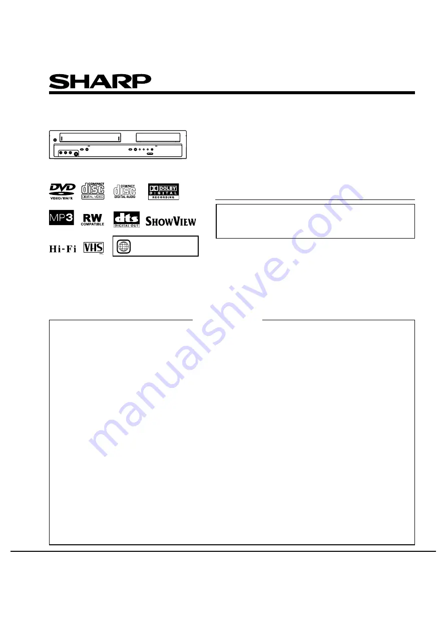
background image

SERVICE MANUAL

DVD-RW RECORDER &
VHS VIDEO CASSETTE RECORDER

MODEL

DV-RW260S

In the interests of user-safety (Required safety regulations

in some countries) the set should be restored to its original

condition and only parts identical to those specified be used.

CONTENTS

SHARP CORPORATION

IMPORTANT WARING .................................................................................................................................................
SERVICING NOTICES ON CHECKING ......................................................................................................................
HOW TO ORDER PARTS ............................................................................................................................................
DISC REMOVAL METHOD AT NO POWER SUPPLY ...............................................................................................
TAPE REMOVAL METHOD AT NO POWER SUPPLY ..............................................................................................
PARENTAL CONTROL-RATING LEVEL ....................................................................................................................
TRAY LOCK .................................................................................................................................................................
GENERAL SPECIFICATIONS .....................................................................................................................................
DISASSEMBLY INSTRUCTIONS ................................................................................................................................
KEY TO ABBREVIATIONS ..........................................................................................................................................
SERVICE MODE LIST .................................................................................................................................................
PREVENTIVE CHECKS AND SERVICE INTERVALS ...............................................................................................
WHEN REPLACING EEPROM (MEMORY) IC ...........................................................................................................
WHEN REPLACING NEW DVD LOADER ..................................................................................................................
RE-WRITE FOR DVD FIRMWARE ..............................................................................................................................
SERVICING FIXTURES AND TOOLS .........................................................................................................................
PREPARATION FOR SERVICING ..............................................................................................................................
MECHANICAL ADJUSTMENTS ..................................................................................................................................
ELECTRICAL ADJUSTMENTS ....................................................................................................................................
TROUBLESHOOTING GUIDE .....................................................................................................................................
BLOCK DIAGRAMS .....................................................................................................................................................
PRINTED CIRCUIT BOARDS ......................................................................................................................................
SCHEMATIC DIAGRAMS ............................................................................................................................................
WAVEFORMS ..............................................................................................................................................................
EXPLODED VIEW ........................................................................................................................................................
REPLACEMENT PARTS LIST .....................................................................................................................................

Page
A1-1
A1-1
A1-1
A1-2
A1-2
A1-2
A1-3
A2-1
B1-1
C1-1
C2-1
C3-1
C4-1
C4-3
C5-1
D1-1
D1-1
D2-1
D3-1
E-1
F-1
G-1
H-1
I-1
J1-1
K1-1

S55J9DV-RW260

The region number

for this recorder is 2

.

2

Summary of Contents for DV-RW260S

Page 1: ...TING LEVEL TRAY LOCK GENERAL SPECIFICATIONS DISASSEMBLY INSTRUCTIONS KEY TO ABBREVIATIONS SERVICE MODE LIST PREVENTIVE CHECKS AND SERVICE INTERVALS WHEN REPLACING EEPROM MEMORY IC WHEN REPLACING NEW DVD LOADER RE WRITE FOR DVD FIRMWARE SERVICING FIXTURES AND TOOLS PREPARATION FOR SERVICING MECHANICAL ADJUSTMENTS ELECTRICAL ADJUSTMENTS TROUBLESHOOTING GUIDE BLOCK DIAGRAMS PRINTED CIRCUIT BOARDS SCH...

Page 2: ...seals on the cabinet chassis and parts Make sure to keep the indications and notices in the operation manual PERFORM A SAFETY CHECK AFTER SERVICING 4 Confirm that the screws parts and wiring which were removed in order to service are put in the original positions or whether there are the portions which are deteriorated around the serviced places serviced or not Check the insulation between the ant...

Page 3: ...e of the Front Cabinet as shown by the arrow Refer to Fig 1 The Tray is opened Draw the Tray DISC REMOVAL METHOD AT NO POWER SUPPLY Fig 1 Front Cabinet DVD Flap Fig 1 Insert hole for screw driver Fig 2 Main Cam Clutch Ass y Main Chassis Front Side Loading Motor Capstan DD Unit Pinch Roller Cam Screw PARENTAL CONTROL RATING LEVEL 4 DIGIT PASSWORD CANCELLATION If the stored 4 digit password in the R...

Page 4: ...CLOSE key on the front panel to check the Tray Lock setting 1 2 3 4 5 NB No indications on the screen when the Tray Lock is setting To unlock the Tray Lock please follow the steps below NB No indications on the screen when the Tray Lock is setting Turn Unit ON Press and hold the 0 key on the remote control unit Simultaneously press and hold the STOP key on the front panel Hold both keys for more t...

Page 5: ...assette E 180 Forward Reverse NTSC or PAL M SP LP 3x 5x Picture Search PAL or SECAM SP LP 5x 7x 7x 13x Frame Advance Yes Slow Speed 1 5 1 10 1 30 G 4 Tuning Broadcasting System CCIR B G OIRT D K System Tuner and System 1Tuner Receive CH Destination Oscar w HYPER CH Coverage Intermediate Picture FP 38 9 MHz Frequency Sound FS 33 4 32 4 MHz FP FS 5 5 6 5 MHz Auto Tuning Method ALL BAND Not Only C C ...

Page 6: ... ohm VCR 0dBm 0 775Vrms Output Level Line Digital Output Level 0 5 V p p 75 ohm DVD S N Ratio at Weighted 90dB DVD Video 42dB VCR at SP Harmonic Distortion 1KHz Typical 0 06 DVD Video 1 5 VCR at SP Frequency Response DVD Mode at DVD 4 Hz 22 kHz DVD Mode at VideoCD SVCD 4 Hz 20 kHz DVD Mode at CD 4 Hz 20 kHz VCR Mode at SP 100 Hz 10 kHz VCR Mode at LP 100 Hz 5 kHz VCR Mode at SLP Hi Fi Audio Signal...

Page 7: ... Yes Display Call On Off Yes AV Setup Yes Video Yes TV Screen Yes Still Mode Yes No Noise Background Yes Brightness Yes DVD Output Yes AV2 Yes AV3 Input Yes Color System No Audio Yes DRC Dynamic Range Control Yes Virtual Surround Spatializer N 2 2 Yes External Audio Input Selection Yes NICAM Yes DOLBY DIGITAL OUTPUT Yes Rec Setup Yes Initial Rec To Yes Initial Rec Mode Yes Auto Chapter Yes Index P...

Page 8: ...me Disc Yes Genre No Play List No Play No Chapter No Rename Title No Delete Playlist No Title Combine No Title Divide No Edit Title No Dubbing DVD VCR Yes VCR DVD Yes Disc Information Yes Disc Type Yes Disc Remain Time Yes Open Yes Close No No disc Yes Reading Yes DVD Mode Yes Play Yes Pause Still Yes Stop Yes Prohibit Mark Yes Step Yes Skip Yes Skip Yes Random Yes CD Video CD SVCD Repeat Yes Slow...

Page 9: ...splay Type 6Digit Fluorescent Indicator Clock Yes 24h AM No PM No Counter VCR Yes hour min sec DVD Yes hour min sec CD Yes min sec TV VIDEO Yes CD Yes DVD Yes VR Mode Yes Video Mode No DVD R Yes DVD RW Yes DVD R No DVD RW No DVD RAM No Disc In Yes Tape In Yes T Rec Yes XP Yes SP Yes LP Yes SLP Yes EP No VP No Counter Remain No Chapter No Title No Track No Yes Repeat A B All No Play VCR Side Yes Pa...

Page 10: ... Yes DISPLAY CALL Yes TOP MENU TITLE LIST Yes UP CH Yes DOWN CH Yes LEFT TRACKING Yes RIGHT TRACKING Yes SELECT ENTER Yes DVD MENU Yes SETUP Yes STOP Yes PLAY Yes PAUSE STILL STEP Yes SKIP INDEX Yes SEARCH REW Yes SEARCH F FWD Yes SKIP INDEX Yes ONE TOUCH REPEAT Yes CM SKIP Yes SLOW No SLOW Yes REC OTR Yes REC MODE SPEED Yes DUBBING Yes AUDIO AUDIO SELECT Yes MARKER No ZOOM Yes REPEAT A B Yes ZERO...

Page 11: ... No Tray Lock Yes One Touch Repeat Yes S Video Output SCART1 DVD Only Yes Audio DAC 192kHz 24bit Features Auto Head Cleaning No VCR Index Search Yes Forward Reverse Picture Search Yes SQPB PAL SP Mode Only No Rec End Search No CS Easy No G 16 Accessories Owner s Manual Yes Language German English Swedish w Guarantee Card No Remote Control Unit Yes Dew Caution Sheet No Battery Yes UM size x pcs UM ...

Page 12: ... Speaker No VHF UHF Antenna Input Output DIN Type AC Inlet No Indicator LED Power No Rec No T Rec No TV VCR No DVD Yes GREEN VCR Yes AMBER Surround No Level Meter No G 18 Set Size Approx W x D x H mm 430 x 309 x 89 5 G 19 Weight Net Approx 5 0 kg 11 0 lbs Gross Approx 6 5 kg 14 3 lbs G 20 Carton Master Carton No Content Sets Material Dimensions W x D x H mm Description of Origin Gift Box Material ...

Page 13: ... time slide in direction of arrow B Then lift in direction of arrow C 1 2 FLAP Refer to Fig 1 2 Fig 1 1 1 1 1 1 A 2 B 1 Top Cabinet Front Cabinet 2 2 2 2 2 3 Operation 1 PCB C 2 3 3 Fig 1 2 A Flap B C 2 NOTE After the set assembling perform the following process so that the wires don t touch to the heating parts 1 2 3 Bind the CD7304 CD504 and Fan motor cable at the Fig 1 position and fix them Pas...

Page 14: ... screws 1 Disconnect the following connector CP506 Remove the Fan Motor in the direction of arrow A Remove the 3 screws 2 Disconnect the following connector CP1701 Remove the Power PCB in the direction of arrow B Fig 1 4 1 5 VCR DECK Refer to Fig 1 5 Do not remove the cable at the FE Head section The FE Head may be damaged if you remove the cable by force NOTE 1 2 3 4 5 6 7 Unlock the 2 supports 1...

Page 15: ...CR PCB Refer to Fig 1 6 1 2 3 4 5 6 Remove the screw 1 Remove the screw 2 Remove the 3 screws 3 Unlock the support 4 Remove the Jack Shield Remove the VCR PCB in the direction of arrow 1 VCR PCB 2 Bottom Plate 3 3 Jack Shield Fig 1 6 3 4 ...

Page 16: ...Top Bracket Top Bracket Main Chassis Main Chassis Cassette Side L Cassette Side R Locker R Fig 2 2 Link Unit 2 3 LINK UNIT Refer to Fig 2 3 Set the Link Unit to the Eject position Unlock the support 1 Remove the A side of the Link Unit first then remove the B side 1 2 3 Fig 2 3 A Link Unit Main Chassis 1 Link Unit B Main Chassis 1 1 NOTE 1 After the installation of the Top Bracket bend the support...

Page 17: ...4 Tension Band Tension Arm Ass y 3 1 Tension Holder Tension Connect NOTE 1 2 3 In case of the Tension Band installation note the direction of the installation Refer to Fig 2 6 C In case of the Tension Band installation install correctly as Fig 2 6 D In case of the Tension Connect installation install as the circled section of Fig 2 6 E Tension Band Tension Connect Tension Connect OK NG Fig 2 6 E T...

Page 18: ...loves Refer to Fig 2 8 A Do not adhere the stains on it When you install the reel clean the shaft and grease it FG 84M If you do not grease noise may be heard in FF REW mode After installing the reel adjust the height of the reel Refer to MECHANICAL ADJUSTMENT 1 2 3 4 5 6 Fig 2 8 A S Reel 1 A T Reel A 1 Idler Arm Ass y Idler Gear NOTE 1 2 In case of the S Reel and T Reel installation check if the ...

Page 19: ...n the screw 3 1 2 3 2 9 CASSETTE OPENER PINCH ROLLER BLOCK P5 ARM ASS Y Refer to Fig 2 9 A Unlock the support 1 and remove the Cassette Opener Remove the Pinch Roller Block and P5 Arm Ass y 1 2 Fig 2 9 A 1 Cassette Opener P5 Arm Ass y Pinch Roller Block Main Chassis NOTE Do not touch the Pinch Roller Use gloves In case of the Pinch Roller Block and the Pinch Roller Cam installation install correct...

Page 20: ... DD Unit Capstan Belt Fig 2 13 1 2 Capstan Holder 2 2 Fig 2 14 A NOTE In case of the Pinch Roller Cam and Main Cam installation install them as the circled section of Fig 2 14 B so that the each markers are met Refer to Fig 2 14 B 2 14 Remove the E Ring 1 then remove the Main Cam Remove the E Ring 2 then remove the Pinch Roller Cam and Joint Gear 1 2 MAIN CAM PINCH ROLLER CAM JOINT GEAR Refer to F...

Page 21: ...stallation install correctly as the circled section of Fig 2 17 C 1 2 3 A OK NG B P4 Cap Cassette Opener Fig 2 17 B Fig 2 17 C Cassette Guide Post Cassette Guide Post 2 16 Remove the Polyslider Washer 1 Remove the Clutch Ass y and Ring Spring Remove the Clutch Lever Remove the Coupling Gear Coupling Spring and Clutch Gear 1 2 3 4 Fig 2 16 A 1 Clutch Ass y Coupling Gear Clutch Lever Ring Spring Cou...

Page 22: ...using a blower type IC desoldering machine Refer to Fig 3 2 2 Fig 3 2 NOTE Do not add the rotating and the back and forth directions force on the IC until IC can move back and forth easily after desoldering the IC leads completely When IC starts moving back and forth easily after desoldering completely pickup the corner of the IC using a tweezers and remove the IC by moving with the IC desoldering...

Page 23: ...3 8 Thin tip Soldering Iron NOTE When the IC leads are bent during soldering and or repairing do not repair the bending of leads If the bending of leads are repaired the pattern may be damaged So always be sure to replace the IC in this case Finally confirm the soldering status on four sides of the IC using a magnifying glass Confirm that no abnormality is found on the soldering position and insta...

Page 24: ...lop Frequency Generator Front Loading Switch Frequency Modulation Frequency Sub Carrier Forward Generator Ground High Pass Filter I K L M N O P R S H SW Hz IC IF IND INV KIL L LED LIMIT AMP LM LDM LP L P F LUMI M MAX MINI MIX MM MOD MPX MS SW NC NR OSC OPE PB PB CTL PB C PB Y PCB P CON PD PG P P R REC REC C REC Y REEL BRK REEL S REF REG REW REV RVS RF RMC RY S CLK S COM S DATA SEG SEL SENS SER SI ...

Page 25: ...tor Separation Transistor Tracking Trick Playback Test Point Unregulated Volt Voltage Controlled Oscillator Video Intermediate Frequency Vertical Pulse Voltage Display Video Playback Variable Resistor Video Recording Visual Search Fast Forward Visual Search Rewind Voltage Super Source Vertical Synchronization Voltage Tuning Crystal Luminance Chrominance C1 2 ...

Page 26: ...P 2 2 sec DVD mode No disc Set Key Operations CH UP PLAY REC total hours are displayed on the TV Monitor Refer to the PREVENTIVE CHECKS AND SERVICE INTERVALS CONFIRMATION OF HOURS USED Can be checked of the INITIAL DATA of MEMORY IC Refer to the WHEN REPLACING EEPROM MEMORY IC Set Key FF 2 sec CH UP PLAY 2 sec Initialization of the factory on VCR NOTE If you set a factory initialization the memori...

Page 27: ...it Clean those parts in contact with the tape Clean the rubber and parts which the rubber touches Replace when rolling becomes abnormal Clean the Head T Brake Band Clutch Ass y Idler Arm Ass y C3 1 CONFIRMATION OF HOURS USED PLAY REC total hours can be checked on the screen Total hours are displayed in 16 system of notation NOTE If you set a factory initialization the total hours is reset to 0 1 2...

Page 28: ...below Audio Control Head 2 TAPE RUNNING SYSTEM When cleaning the tape transport system use the gauze moistened with isopropyl alcohol 3 CYLINDER Wrap a piece of chamois around your finger Dip it in isopropyl alcohol Hold it to the cylinder head softly Turn the cylinder head counterclockwise to clean it in the direction of the arrow Refer to the figure below NOTE Do not exert force against the cyli...

Page 29: ...ugh the ADDRESS until required ADDRESS to be changed is reached Press ENTER to select DATA When DATA is selected it will blink Again step through the DATA using Tracking or button until required DATA value has been selected Pressing ENTER will take you back to ADDRESS for further selection if necessary Repeat steps 4 to 7 until all data has been checked When satisfied correct DATA has been entered...

Page 30: ...ing Channel button or the following buttons below Numbers are 10 keys from 0 to 9 Alphabets are A VCR EJECT B DVD OPEN CLOSE C DVD VCR D TIMER REC E INPUT SELECT F DISPLAY Press ENTER to select DATA Again step through the DATA using Channel or button until required DATA value has been selected Pressing ENTER will take you back to ADDRESS for further selection if necessary Repeat steps 4 to 7 until...

Page 31: ...gion No Turn on the POWER and set to the DVD mode Press both CH DOWN button on the set and the DVD VCR button on the set for more than 2 seconds Information screen will be displayed on the TV Monitor Refer to Fig 1 If the writing Region No is appeared the Region setting is completed Turn off the power 1 2 3 4 5 6 7 8 9 10 11 WHEN REPLACING NEW DVD LOADER NOTE If a service repair is undertaken wher...

Page 32: ...the screen the writing will be finished NOTE Do not turn off the unit on the way or push the tray by hand to close it Up Date error will happen and can not be done with the Up Date of Up Date Disc Unplug the AC cord then plug it in After the write set to the initializing of shipping Turn on the POWER and set to the DVD mode Press both CH UP button on the set and the PLAY button on the set for more...

Page 33: ...r Plane Reel Disk Height Adjustment Jig Torque Tape VHT 063 VSR Torque Brake Torque S Reel T Reel Ass y Monoscope 6KHz For 2 head 1 speed model 4 head model Color Bar 1KHz For 2 head 1 speed model 4 head model Hi Fi Audio For Hi Fi model X Value Adjustment For 2 head 1 speed model 4 head model Monoscope 6KHz For 2 head 2 speed model Color Bar 1KHz For 2 head 2 speed model X Value Adjustment For 2 ...

Page 34: ...0 mm Adjust the other reel in the same way Master Plane JG022 Reel Disk Height Adjustment Jig JG024A Fig 1 1 A Fig 1 1 B 1 2 CONFIRMATION AND ADJUSTMENT OF TENSION POST POSITION 1 2 3 Set to the PLAY mode Adjust the adjusting section for the Tension Arm position so that the Tension Arm top is within the standard line of Main Chassis While turning the S Reel clockwise confirm that the edge of the T...

Page 35: ...to the Stop mode While unplug the AC cord when the Pinch Roller Block is on the position of Fig 1 4 A Move the Idler Ass y from the T Reel Install the Torque Gauge JG002E and Adapter JG002B on the T reel Turn the Torque Gauge JG002E counterclockwise Then confirm that it indicates 30 50gf cm Fig 1 4 A The position at FF mode Stop at this position The position at STOP mode Capstan DD Unit Cassette H...

Page 36: ...de Roller Refer to item 2 1 Confirm and adjust the Audio Control Head Refer to item 2 2 Connect CH 1 of the oscilloscope to TP102 CH 2 to TP103 and CH 3 to HOT side of Audio Out Jack Playback the VHS Alignment Tape JG001U or JG001V Refer to SERVICING FIXTURE AND TOOLS Press and hold the Tracking Auto button on the remote control more than 2 seconds to set tracking to center Set the X Value adjustm...

Page 37: ...NT PARTS LOCATION GUIDE 1 2 3 4 5 6 7 8 9 10 1 Tension Connect 2 Tension Arm 3 Guide Roller 4 Audio Control Head 5 X value adjustment driver hole 6 7 8 9 10 P4 Post T Brake Spring T Reel S Reel Adjusting section for the Tension Arm position D2 4 ...

Page 38: ... alignment tape JG001E Press and hold the Tracking Auto button on the remote control more than 2 seconds to set tracking to center Press both CH UP button on the set and the STOP button on the set for more than 2 seconds 1 2 3 4 When you exchange IC and Transistor for a heat sink apply the silicon grease YG6260M on the contact section of the heat sink Before applying new silicon grease remove all ...

Page 39: ...ECK CD FE HEAD CD651 CP502 CP7301 CP7304 CD7304 VCR PCB CD502 CD7301 CD7302 CD7303 J653 J652 J651 V651 TP103 CP8303 TP651 OS651 CP8302 J654 CP651 CP102 TU301 J8002 TP102 CP103 AC HEAD CD102 CP506 CP504 CD501 FAN MOTOR CP7302 CP7303 CP4001 S502 S501 CD4001 CP1703 CP1701 J8001 J8003 CP654 CP8001 CD691 CP681 OPERATION 2 PCB CP8304 CD8001 AC IN ...

Page 40: ...eck of T501 and peripheral circuit Is the voltage at pin 29 of IC 3001 0V Does display light Is the voltage linked to L506 THE POWER SUPPLY CUT Inserting a cassette and push play button YES YES NO NO Does the power cut after 3 seconds Check CAPSTAN DD UNIT and CYLINDER UNIT Does the power cut after about 6 seconds Check Q3006 Q3008 and CAPSTAN BELT Check the POWER BLOCK ...

Page 41: ...e at pin 8 of CP3001 about DC12 6V Check IC502 In playback is at pin 12 of CP3001 about DC2 6V YES YES YES NO NO NO AUDIO SHAKES Is AUDIO HEAD scratched Change AUDIO HEAD At playback is input about 4 5Vp p of a rectangular wave at pin 9 of IC3001 Change CAPSTAN DD UNIT Check IC3001 At playback is pin 5 of CP3001 3 5V Check AUDIO BLOCK ...

Page 42: ...e CASSETTE TAPE CAN NOT BE INSERTED Check WORM GEAR of cassette loading block YES YES YES NO NO NO Does WORM GEAR of cassette loading block move When a CASSETTE can not inserted is pin 25 of IC3001 5V When a CASSETTE is inserted is pin 8 of CP3001 12 6V Check circuit of POWER BLOCK ...

Page 43: ...loading block YES YES YES NO NO NO Does SW3001 and REC LEVER correctly set After inserting CASSETTE is pin 51 of IC3001 0V Correctly SW3001 and REC LEVER set WHEN INSERTING A CASSETTE IT EJECTS IMMEDIATELY Check DECK MECHANISM CAN NOT FF REW YES NO At FF REW does voltage at pin 98 of IC3001 change Check of IC3001 ...

Page 44: ...DIATELY Check POWER BLOCK Change IC3001 Check Q3006 and Q3008 YES YES YES YES YES NO NO NO NO NO Does CYLINDER rotate Is there HEAD SW PULSE at TP102 Is the voltage at pin 2 of CP3001 12V At play is the voltage at pin 12 of CP3001 2 6V Is PG PULSE signal inputted to pin 104 of IC3001 ...

Page 45: ...PICTURE JITTERS VERTICAL MINUTELY Is FG wave of CP3001 at pin 11 5V Is pin 12 of CP3001 2 6V AUTO TRACKING DOES NOT OPERATE 2 5Vp p YES YES NO NO In auto tracking is the voltage at pin 24 of IC3001 more than DC 0 2V Does the CTL pulse signal about 2 5Vp p appear at pin 7 of IC3001 Check CONTROL HEAD Change IC3001 ...

Page 46: ...O WHEN PLAYBACK FF OR REW MODE IS ACTIVE UNIT STOPS IMMEDIATELY Does CAPSTAN DD MOTOR rotate Refer to section CAPSTAN DD MOTOR NOT ROTAING Is there REEL SENSOR PULSE signal at pin 69 and pin 70 of IC3001 Check Q3001 and Q3002 Change IC3001 ...

Page 47: ... on the picture appear By adjusting the MANUAL TRACKING UP DOWN BUTTONS will the line disappear Check P B ENVELOPE Is a height of GUIDE POST maximum The height of GUIDE POST readjust Is PG SHIFTER adjustment 6 5H Adjust PG SHIFTER Is a wave of PB Y unusual Change IC101 and peripheral circuit Change IC101 NO ...

Page 48: ...AYBACK THE PICTUER DOES NOT APPEAR Does E E picture appear Refer to AT E E NO PICTURE Is there video signal of IC101 at pin 29 Change IC101 Change IC8005 Is there video signal of IC8005 at pin 2 Is there video signal of IC101 at pin 29 Check J8001 Change IC101 ...

Page 49: ... IC101 at pin 26 Change IC101 Change IC8006 Is there video signal of IC8006 at pin 7 Is there video signal of IC3001 at pin 16 17 Check IC8006 and peripheral circuit YES NO Is there video signal of IC101 at pin 15 Check J8001 and peripheral circuit Check J8001 YES NO Is there video signal of IC3001 at pin 19 Change IC3001 Check J8001 pin 19 and peripheral circuit ...

Page 50: ...signal at pin 26 of IC101 Change X tal Change IC101 YES NO Is there color signal in video signal at pin 7 of IC8006 Change IC8006 YES NO Is there color signal in video signal at pin16 17 of IC3001 Check IC8006 and peripheral circuit YES NO Is there color signal in video signal at pin19 of IC3001 Change IC3001 Check J8001 pin 19 and peripheral circuit ...

Page 51: ...nal at pin 26 of IC101 Check CYLINDER YES NO Is noisy a wave of video signal at pin 7 of IC8006 Change IC8006 YES NO Is noisy a wave of video signal at pin 16 17 of IC3001 Check IC8006 and peripheral circuit YES NO Is noisy a wave of video signal at pin 19 of IC3001 Change IC3001 Check J8001 and peripheral circuit ...

Page 52: ... AT PLAYBACK THE COLOR DOES NOT APPEAR Change IC101 YES YES YES NO NO NO AT PLAY AUDIO DOES NOT APPEAR At E E does audio appear Refer to section AT E E NO SOUND Is the voltage at pin 96 of IC101 about 2 5V Check A C HEAD Change IC101 and check peripheral circuit of pin 6 of IC101 Is there audio signal at pin 6 of IC101 Check whether there are not a damage dirt in AUDIO HEAD and peripheral circuit ...

Page 53: ...E 14 YES YES NO NO CAPSTAN DD MOTOR NOT ROTATING Check POWER BLOCK Change IC3001 In playback is there voltage at pin 78 of IC3001 2 5V DD MOTOR rotate now If not replace it In playback is there voltage at pin 2 of CP3001 12V ...

Page 54: ...t pin 98 of IC101 Check POWER BLOCK and voltage of base of Q103 Check disconnection and short of L102 Is there audio signal at pin 1 of IC101 Is there voltage of base of Q103 about 5V Check IC701 and the circuit from TUNER or audio input jack to IC701 Change Q103 Change L101 Is there a sine wave at pin 6 of L101 Check lead wire of A C HEAD and CONNECTOR ...

Page 55: ...LATION DEPARTMENT Check IC3001 YES YES YES YES NO NO NO NO RECORDING MECHANISM WORKS BUT NO VIDEO RECORD FROM INPUT JACK OR TUNER Is there video signal at pin 15 21 of IC 101 Is the BASE of Q103 5V Is the voltage at pin 96 of IC3001 5V Check circuit of video signal from VIDEO IN or TUNER to IC101 Change IC3001 Change IC101 Is there video signal at pin 26 of IC101 Check CYLINDER UNIT and circuit ar...

Page 56: ...ality AUDIO JACK CONNECT Connection is done over again Is there audio signal at pin 78 80 of IC701 Check J8001 and peripheral circuit Change IC701 Is there audio signal at pin 9 11 72 74 of IC701 Check J8001 J651 J652 and peripheral circuit Is there audio signal of J8001 at pin 1 3 ...

Page 57: ...STEREO appear Is the voltage at pin 92 of IC101 5V Refer to section E E AUDIO STEREO DOES NOT APPEAR Check POWER BLOCK Is the voltage at pin 95 of IC3001 5V Change IC3001 Check J8001 Change IC701 Is there audio signal at pin 11 74 of IC701 Is there audio signal at pin 6 of IC701 Check circuit around of J8001 ...

Page 58: ...S NOT APPEAR Is the voltage at pin 5 15 36 46 of IC701 5V Is the voltage at pin 3 of IC701 9V Check POWER BLOCK Check POWER BLOCK Change IC701 Is there Audio signal at pin 11 14 of IC701 Is there Audio signal at pin 78 80 of IC701 Check circuit around of J8001 Check J651 J652 ...

Page 59: ...es E E AUDIO MONO appear Refer to section E E AUDIO MONO DOES NOT APPEAR Check circuit around of TU301 at pin 16 Change IC701 Check IC8001 Is there signal at pin 48 of IC701 Is there audio signal at pin 78 80 of IC701 Is there audio signal at pin 41 44 of IC8001 Check circuit around of J8001 ...

Page 60: ...fer to section E E AUDIO STEREO DOES NOT APPEAR Does E E AUDIO STEREO appear At the time of channel change does the display of a stereo come out to the screen Is there audio signal at pin 2 of IC801 Check circuit around of TU301 Change IC701 Check IC8001 Is there audio signal at pin 41 44 of IC8001 Check circuit around of J8001 Change IC701 Is there audio signal at pin 78 80 of IC701 ...

Page 61: ...O appear Does NORMAL PB AUDIO appear Is there audio signal at pin 24 27 of IC701 Is there audio signal at pin 78 80 of IC701 Check circuit around of J8001 Refer to section E E AUDIO STEREO DOES NOT APPEAR Refer to section AT PLAY AUDIO DOES NOT APPEAR Check circuit of HEAD AMP and CYLINDER UNIT Change IC701 ...

Page 62: ... state of video recording is there audio signal at pin 11 and 74 of IC701 Is there audio signal at pin 78 80 of IC701 At recording and play is there signal at pin 7 8 and 9 of CP101 Check IC701 Check CYLINDER UNIT Change IC701 Check circuit around of J651 J652 Refer to section E E AUDIO MONO DOES NOT APPEAR ...

Page 63: ...heck CD504 connection to CP504 and DECK Check DECK DVD SECTION E E DOES NOT APPER AT DVD MODE No Yes No Yes No Yes Check VCR block Check IC4001 and peripheral circuit Check IC4009 and peripheral circuit Check VCR block Is there a signal in at pin 97 107 108 117 118 and 127 of IC4001 with each output mode Is there a signal in at pin 2 4 9 and 207 of IC4009 Is there a signal in at pin 17 and 19 of C...

Page 64: ... at pin 9 11 13 and 15 of CP7301 with each input No Yes Is there a signal in at pin 1 22 and 28 of IC7303 and 56 100 and 110 of IC4001 Check IC7303 IC4009 IC4010 and peripheral circuit Go to NO AUDIO ON PLAYBACK No Yes Check IC7301 and peripheral circuit Is there a signal in at pin 7 and 8 of IC7301 No Yes Check IC7304 and peripheral circuit Is there a signal in at pin 1 and 7 of IC7304 ...

Page 65: ...1 Is there a signal in at pin 5 and 7 of CP7301 with each input No Yes Is there a signal in at pin 1 22 and 28 of IC7303 and 56 100 110 of IC4001 Check IC7303 IC4009 IC4010 and peripheral circuit Go to NO AUDIO ON PLAYBACK No Yes Check IC7301 and peripheral circuit Is there a signal in at pin 7 and 8 of IC7301 No Yes Check IC7304 and peripheral circuit Is there a signal in at pin 1 and 7 of IC7304...

Page 66: ...s the waveform at pin 25 of IC8001 No Yes Check IC8001 and peripheral circuit Check J8001 and peripheral circuit NO PLAYBACK PICTURE OF S VIDEO JACK Is there Y signal at pin 118 of IC4001 Yes No Check CP7302 connection to CP8302 Yes No Check IC4001 and peripheral circuit Is there Y signal at pin 12 of CP8302 Check J8001 and peripheral circuit Check IC8004 and peripheral circuit Yes No Is there Y s...

Page 67: ...rcuit Is there C signal at pin 8 of CP8301 Is there C signal at pin 127 of IC4001 Check CP7302 connection to CP8301 Check J8001 and peripheral circuit Check IC8009 and peripheral circuit Yes No Is there C signal at pin 2 of IC8009 Check IC8003 and peripheral circuit Yes No Is there C signal at pin 2 of IC8003 ...

Page 68: ... Yes No Is there Y signal at pin 2 of IC8008 Check IC8008 and peripheral circuit NO COLOR PLAYBACK PICTURE OF YUV JACK Yes No Yes No Check IC4001 and peripheral circuit Is there U V signals at pin 16 and 18 of CP8302 Is there U V signals at pin 97 and 107 of IC4001 Check CP7302 connection to CP8302 Check J8003 and peripheral circuit Yes No Is there U signal at pin 2 of IC8012 and V signal 2 of IC8...

Page 69: ... Yes Check VCR block VIDEO CAN NOT RECORD TO DVD Is there a signal in at pin 17 and 19 of CP7301 and at pin 1 and 19 of CP7302 with each input No Yes Check IC4009 DVD DECK and peripheral circuit Is there a signal in at pin 79 98 128 and 142 of IC4001 No Yes Check IC7302 and peripheral circuit Is there a composite signal in at pin 4 of IC4009 No Yes Check IC4001 DVD DECK and peripheral circuit Is t...

Page 70: ...1 13 and 15 of CP7301 with each input No Yes Check IC7301 and peripheral circuit Is there a signal in at pin 7 and 8 of IC7301 No Yes Check IC7303 and peripheral circuit Is there a signal in at pin 177 and pin 181 to 183 of IC4009 No Yes Check IC4001 DVD DECK and peripheral circuit Is there a signal in at pin 1 2 and 3 of IC7301 ...

Page 71: ...DMARQ MLINK I2C EN ATCS SEL ATCS SEL EN IC7303 32MBIT FLASH SCL SDA 27M OSC VIDEO OUT DATA LINE RAMDAT16 31 RAMBA0 1 RAMADD0 12 RAMDQM RAMWE PCLK RAMCAS RAMRAS RAMCS VIDEO IN SEL CVBSIN CVBS OUT YUV Y C A 1 8V C D5V F P CON D5V E P CON 12V D A5V B 3 3V AMCLK SEL B SN74LVC1G125DCKR IC4010 AMCLK SW 2 4 1 MPEG DATA IN MPEG DATA OUT VADDIS INT MPEG CS MPEG CLK SCL SDA RAMDAT0 15 FRAMBA0 1 FRAMADD0 1 F...

Page 72: ...COM EP LP CH2 L CP101 4 5 6 7 8 9 SP CH1 R SP_COM SP CH2 L HF1 R HF_COM HF2 L 2 AE HEAD 1 FE HEAD GND CP103 2 FE HEAD HOT TU_VIDEO_OUT 89 85 Y C_VIDEO_OUT REC MUTE MAIN DE EM FM AGC 629 TRAP 69 71 X101 4 433619MHz XTAL VCO OSC P REC Fillter NL E MPH DEM HPF DLIM DEM0 P R Y LPF N L DE EM 33 35 GCL 37 GCL LPF 38 Y CCD 49 51 36 YLR REC DO DO 29 V AMP SQUELCH Clear SYNC V FBC VALC P R 28 V FBC VALC 23...

Page 73: ...IN OUT TUINER HI FI VADDIS_RESET VADDIS INT 44 KEY A 30 45 KEY B 29 MPEG_RESET NADDIS INT KEY A KEY B FL_CLK REM IN 43 48 FL_CLK REM_IN FL_DATA 49 FL_DATA FL_CS 47 FL_CS CYL _CTL 2 3 4 1 2 3 4 1 REEL SENS Q3002 REEL SENS Q3001 REEL T 70 REEL S 69 2 3 4 1 P CON 5V 59 60 MPEG_DATA 40 MPEG_CLK CH_A_MUTE H VADDIS D OUT VADDIS IIC SDA VADDIS IIC CLK CH A MUTE L VADDIS D IN AUDIO_MUTE H V REC ST H 71 V ...

Page 74: ...707 M CON POWER SW Q1712 AT 12V REG IC1704 KIA78R12API P CON 12V REG IC1705 KIA78R12API 8V REG Q1703 POWER SW Q1713 P CON 3 3V REG IC1701 BA00BC0WT V5 4 1 2 4 1 2 1 3 4 2 P CON 1 8V REG IC1706 BA00BC0WT V5 4 1 2 MPEG SW Q1714 H VOLT CTL Q1709 HEATER SW Q1710 P CON 8V P CON 5V AT 12 6V CAP_VCO OPERATION DISPLAY SYSCON MPEG P CON 5V AT 5V M CON MPEG 5V ON H AT 5 2V VCR_P_ON L MP_P CON 1 8V MP_P CON ...

Page 75: ...A FRONT_A_IN_R FRONT_A_IN_L FRONT_V_IN REGULATOR SYSCON AV IN OUT TUNER HI FI GND KEY B C KEY A DVD LED AT 5 2V 5 3 2 1 CH DOWN OPEN CLOSE SYSCON 43 13 7 9 30 8 F 9 F 10 OPERATION DISPLAY BLOCK DIAGRAM 4 5 3 2 1 4 PLAY SW681 SW682 SW683 SW684 SW685 SW686 SW687 D681 CH UP SW688 4 3 J654 6 1 2 FRONT_Y_IN FRONT_C_IN FRONT_S_SW EJECT DVD VCR SW653 SW651 BUFFER Q652 BUFFER Q651 21PIN IN OUT 1 2 KEY B G...

Page 76: ... HIFI_AUDIO_OUT R HIFI_AUDIO_OUT L DEC_AUDIO R DEC_AUDIO L NORNAL_A_OUT NORNAL_A_IN HIFI_REC MUTE AUDIO_MUTE H HIFI_H SW HF1 HF_COM HF2 DVD_AUDIO L DVD_AUDIO R ST SRESET AFT S CURVE IIC_DATA IIC_CLK SYNC DET FRONT_Y_IN FRONT_C_IN VCR TU_V_IN V PR V OUT 21PIN IN OUT U PB V OUT Y G V OUT DVD_VIDEO_OUT SWD VIDEO 4 16 14 19 7 5 17 TU301 5 6 2 Q8311 BUFFER X802 18 432MHz 31 30 12 13 22 NICAM A2 IC801 M...

Page 77: ...3 REG SW 5 5 2 40 39 Y G V OUT U PB V OUT SPDIF BLAKKING L PERI_CTL_IN 35 21 22 SYSCON 6 4 1 TU DVD VIDEO SW IC IC8002 MM1501XNRE 7 3 1 VIDEO SW IC IC8006 NJM2534V 4 2 7 1 3 VCR TUNER VIDEO SW IC IC8007 NJM2534V 4 2 Q8015 BUFFER CH _V_MUTE H FRONT_V_SW H VCR_DUB H VCR TU_V_IN TU_VIDEO_OUT SWD VIDEO FRONT_V_IN AV IN OUT TUNERT HI FI OPERATION DISPLAY P_MUTE H OSD_VIDEO_OUT Q8004 MUTE SW 19 AT 12V S...

Page 78: ...ER 32V P FAIL DRIVE ON H UNREG 3 3V UNREG 3 3V AT 5 2V AT 5 2V AT 13V MOTOR 12V CP502 REGULATOR 4 1 P CON D5V P CON 12V CP504 DVD LOADER UNIT 18 DRIVE 12V REG IC502 KIA278R12PI 1 2 IC501 KIA431A AT VOLTAGE CTL IC 3 1 3 4 1 2 12 13 16 1 P CON 12V CP506 15 Q505 DRIVE 5V SW FAD MOTOR Q503 SAFTY SW F 15 F 16 4 Q504 SAFTY SW POWER BLOCK DIAGRAM 1 MOTOR 27V 19 ...

Page 79: ...4008 R4108 R4117 R4068 C4009 R7338 C4013 C4100 R4116 C4017 C7307 C4086 C4002 C4088 C4066 C4140 R4093 C7308 C4153 C7340 R4123 C7364 C4012 C4152 R7331 C4139 C4087 R4100 C4110 C4069 C4027 L7302 C7314 C7358 C4033 L7301 C7330 C7312 C4030 C4064 R4017 C7318 C7323 C4065 R7337 R4072 C4045 R7304 C4099 IC4007 C4043 B7305 C4024 R4124 C4021 R4070 C4026 C7315 R4006 C7360 L7308 L 7 3 0 9 C4015 C7303 R4064 R7307 ...

Page 80: ...196 L109 C150 C159 C158 C167 C175 W200 C172 W192 C180 W203 W205 L102 CP102 C181 C119 C116 C134 C135 L110 L112 C176 L108 L111 W282 C152 W319 C106 W125 Q102 C101 C105 L101 W124 W123 W122 W126 R109 R132 W131 W132 L104 W133 C713 W212 W194 W193 L106 R703 C739 W209 W210 W207 W206 W255 W284 W280 W276 W291 W315 W312 W373 W182 W377 W402 R3002 W383 W287 W322 W324 W325 W289 W288 W399 W138 W139 W336 W413 W414...

Page 81: ...9 C3017 C3039 R3006 C651 C3061 R3044 R3045 C3056 C3014 C3063 R3004 Q651 R656 R654 R655 R659 Q652 R657 R658 R663 R664 R652 C670 R670 R669 C666 C667 C668 R667 R3057 Q3007 R666 R3036 R3011 Q1712 Q8305 R8325 R8321 R3015 C675 C676 C736 C731 C722 R714 R713 C728 C726 C721 C734 C738 R721 R720 R715 C740 R716 R701 R704 R705 R702 R706 R712 C711 C108 C122 C123 C124 C112 R111 C110 R107 R104 R114 C129 C143 R122...

Page 82: ...506 CP502 D512 C531_1 L507 R533 D518 R519 D523 C538 C528_1 C505_1 C509 D508 D510 D521 C527 W012 D532 C506 R516 C508_1 C523 D502 D503 D505 D506 W013 W010 R509 C503 C533 HS501_1 T501 D535 D515 C519_3 Q503 R514 R523 Q504 C536 D534 R527 R526 R538 R513 D514 R518 D516 D520 IC502 D507 R534 R535 R539 R529 R517_2 W803 D533 W003 D529 D517 C517_1 C530_1 W001 C522_1 W005 C504 C543 C542 C516 D522 Q506 R510 D51...

Page 83: ... MA11 MBA1 MA9 MD25 MA10 MA8 MA0 MA7 MD22 MA1 MA6 MD26 MA2 MA5 MD21 MA3 MA4 MD27 MD20 MD28 MD19 MD29 MD18 MD16 MD31 MD30 MD17 MD17 MD30 MD18 MD29 MD31 MD16 MD19 MD28 MA3 MD20 MD27 MA4 MA2 MD21 MD26 MD22 MD25 MA5 MA1 MA6 MD23 MD24 MDQM MWE MDQM MCAS MCLK MRAS MCS MA12 MBA0 MA11 MBA1 MA9 MA10 MA8 MA0 MA7 MA10 MA11 MA12 MD10 MD11 MD12 MD13 MD14 MD15 MA1 MA6 MA0 MA7 MA8 MA9 MD7 MD8 MD6 MD9 MD5 MD4 MD3...

Page 84: ... MC P H I L VID5 RAMADD9 VID6 RAMADD8 RESET VID7 RAMADD7 VIDCLK RAMADD6 AOUT0 RAMADD5 ABCLKO RAMADD4 ALRCLKO RAMADD3 ATIOW SCL RAMADD2 ATDD1 VID1 SDA RAMADD1 ATDD5 VID2 ATDD7 VID3 VADDIS_AMCLK RAMADD0 VID4 ADC_ADAT PCLK ML RAMCLE MC RAMDQM MD RAMWE BOOTSEL0 RAMCAS MD DRVRST VID6 RAMRAS VID5 RAMCS VID7 RAMBA0 VID0 ADC_ADAT RAMBA1 I55_AODAT PNVMCE RESET ATIOR ATDD0 ATDD4 ASP1 ATDD6 VIDVLD VID3 VIDHS...

Page 85: ...AMDAT24 RAMDAT23 FRAMADD1 RAMADD2 RAMDAT22 RAMDAT21 FRAMADD0 RAMDAT20 RAMDAT19 FRAMADD10 RAMDAT18 RAMDAT17 FRAMBA1 FRAMDAT16 RAMDAT16 RAMDAT15 FRAMBA0 FRAMDAT17 RAMDAT14 RAMDAT13 FRAMDAT7 FRAMDAT18 RAMDAT12 RAMDAT16 RAMDAT31 RAMDAT11 FRAMDAT6 FRAMDAT19 RAMDAT10 RAMDAT9 RAMDAT17 RAMDAT30 FRAMDAT5 FRAMDAT20 RAMDAT8 RAMDAT7 RAMDAT18 RAMDAT29 FRAMDAT21 RAMDAT6 RAMDAT5 RAMDAT3 FRAMDAT22 RAMDAT4 RAMDAT1...

Page 86: ...081 33 R4083 33 R4068 33 R4094 22 R4093 82 R4085 22 R4092 22 R4084 82 R4091 33 R4090 33 R4088 33 R4089 33 R4087 33 R4086 82 R4064 5 6K R4117 10K R4110 10K DRVRST ATDD7 ATDD8 ATDD6 ATDD9 ATDD5 ATDD10 ATDD4 ATDD11 ATDD3 1 ATDD12 DRVRST ATDMARQ ATDD2 ATIOW 3 ATDD13 ATIOR ATIORDY 4 ATDD1 ATDMACK 5 ATDD14 ATINTRQ ATDA1 6 ATDD0 ATDA0 7 ATDD15 ATCS0 ATDD0 8 ATDD1 9 ATDD2 ATDD3 10 ATDMARQ ATDD4 11 ATDD5 A...

Page 87: ...6 6 8K 1 R7352 15K 1 R7355 100 R7332 1 8K 1 R7324 12K 1 R7353 6 8K 1 R7325 12K 1 R7334 1 8K 1 R7356 680K R7357 100 C7329 10 16V V S C7328 10 16V V S C7350 10 16V V S C7305 10 16V V S C7322 47 6 3V V S C7324 10 16V V S C7385 22 16V V S C7382 100 16V V S C7383 22 16V V S DAC_L ABCLKO AOUT0 ALRCLKO 12V VADDIS_AMCLK DAC_R MD MC ML ADC_ADAT I55_ALRCLK ZERO I55_ABCLK I55_AMCLK I55_ABCLK I55_AMCLK ADC_AD...

Page 88: ...07 75 1 R7304 75 1 R7302 75 1 R7350 75 R7348 75 R7303 75 1 R7313 75 1 R7335 51 R7331 51 R7333 51 R7339 100K R7337 100K R7338 100K R7340 51 R7342 51 R7341 51 R7327 51 R7323 51 R7326 51 C7370 47 6 3V V S C7369 47 6 3V V S C7367 47 6 3V V S BS_AUDIO_L BS_AUDIO_R TU_AUDIO_L ZERO DAC_L TU_AUDIO_R DAC_R BS_AUDIO_L AUDIO_IN_L_2 BS_AUDIO_R TU_AUDIO_L TU_AUDIO_R AUDIO_IN_R_2 AUDIO_IN_L_2 AUDIO_IN_R_2 AUDIO...

Page 89: ...V DET SWD_VIDEO P CON 5V GND NORMAL_AUDIO_IN P CON 5V NORMAL_AUDIO_OUT SP L HF1 SP_COM HF2 HF_COM SP R EP L HF1 EP_COM HF_COM EP R HF2 SP R SP_COM SP L EP R EP_COM EP L SYNC DUMMY_V SYNC P CON 5V CTL CTL Y C_VIDEO_OUT NORMAL_AUDIO_OUT NORMAL_AUDIO_IN V REC_ST H P CON 5V V REC_ST H DVD_VIDEO_OUT TU_VIDEO_OUT P CON 5V P CON 5V SWD_VIDEO H 14 H 13 VCR PCB Y C AUDIO HEAD AMP SECAM SCHEMATIC DIAGRAM NC...

Page 90: ...P_ON L IIC_CLK DUMMY_V SYNC FWE GND MPEG_DATA V_H SW MOTOR_GND MPEG_CLK V REC_ST H AT 12 6_V AUDIO_MUTE H IIC_DATA RESET IIC_CLK CAP_VCO CAP_LIMIT Y C_VIDEO_OUT SYNC BLAKKING L ST_RESET P_MUTE H CAP_FG FRONT_S_SW CAP_F R TAB_SW CAP_LIMIT DRIVE_ON H FL_DATA HIFI_H SW IIC_CLK FL_CLK CONTROL_IN IIC_DATA FL_CS LDM_CTL HIFI_ENV DET CYL_FG PG FIP_ON L HIFI_REC_MUTE CYL_DRIVE MPEG_RESET AUDIO_MUTE H YUV_...

Page 91: ...2013H02 2P 1 2 SWD_AUDIO L SWD_AUDIO R FRONT_AUDIO_IN L P CON 5V C_V_OUT Y_V_OUT SYNC DET FRONT_AUDIO_IN R VCR_DUB H TU_VIDEO_OUT VCR TU_V_IN CH_V_MUTE H TU_VIDEO_OUT OSD_VIDEO_OUT P CON 5V HIFI_AUDIO_OUT L HIFI_AUDIO_OUT R TU_AUDIO L TU_AUDIO R CH_A_MUTE H VCR TU_V_IN FRONT_Y_IN V PR _V_OUT FRONT_C_IN U PB _V_OUT Y_V_OUT Y G _V_OUT DVD_VIDEO_OUT AT 5 2V IIC_DATA C_V_OUT P CON 5V DVD_AUDIO_OUT_L I...

Page 92: ...1504S_Y_RTK MUTE DRIVE Q8008 KTA1504S_Y_RTK BLANKING OUT CAUTION DIGITAL TRANSISTOR L8002 22uH 0305 L8009 100uH 0305 L8008 100uH 0305 L8010 100uH 0305 L8001 22uH 0305 L8012 100uH 0305 L8011 100uH 0305 L8003 100uH 0305 L8005 10uH 0305 L8013 100uH0305 L8014 100uH0305 L8007 10uH L8006 1uH Q8011 KTC3875S_Y_RTK D AUDIO DRIVER Q8013 KTC3875S_Y_RTK BLANKING OUT OF PRINTING AND SUBJECT TO CHANGE WITHOUT N...

Page 93: ...1281_Y M CON 5V SW Q1704 KTA1281_Y MPEG 5V SW CAUTION DIGITAL TRANSISTOR L1702 47uH 0305 Q1709 KTC3203_Y HEATER VOLTAGE CTL Q1708 KTC3209_Y P CON 5V SW Q1703 KTC3209_Y 8V REG Q1701 KTD1691Y 24V REG Q1710 DTA124EKA HEATER SW Q1713 DTA124EKA POWER SW Q1714 DTA124EKA MPEG POWER SW OF PRINTING AND SUBJECT TO CHANGE WITHOUT NOTICE NOTE THIS SCHEMATIC DIAGRAM IS THE LATEST AT THE TIME CAUTION DIGITAL TR...

Page 94: ...D SUBJECT TO CHANGE WITHOUT NOTICE NOTE THIS SCHEMATIC DIAGRAM IS THE LATEST AT THE TIME DURING PLAYBACK MEASURED WITH THE DIGITAL TESTER NOTE THE DC VOLTAGE EACH PART WAS CP654 A2001WV2 2P 1 2 CD691 C3220901 CD651 C3252804 HEATER_DC HEATER_DC HEATER_DC HEATER_DC 1G 2G 3G 4G 5G 6G 7G 8G 9G P10 P11 P12 P1 P2 P3 P4 P5 P6 P7 P8 P9 22V P1 P2 P3 P CON 12V 9G P4 KEY A 8G P5 KEY B REM_IN 7G P6 FL_CS FL_C...

Page 95: ...LATEST AT THE TIME CAUTION DIGITAL TRANSISTOR DURING PLAYBACK MEASURED WITH THE DIGITAL TESTER NOTE THE DC VOLTAGE EACH PART WAS NORMAL_AUDIO_IN NORMAL_AUDIO_OUT HF1 HF2 AUDIO_MUTE H HF_COM TU_AUDIO R TU_AUDIO L AT 5 2V HIFI_H SW IIC_CLK IIC_DATA HIFI_H SW HIFI_ENV DET IIC_CLK HIFI_REC_MUTE AUDIO_MUTE H IIC_DATA DEC_AUDIO R DEC_AUDIO L HIFI_AUDIO_OUT R HIFI_AUDIO_OUT L SWD_AUDIO L DVD_AUDIO_R SWD_...

Page 96: ...16 1SS133 D512 SB340FL 6737 D525 21DQ09N D538 1SS133 D517 1SS133 D506 RM11C EIC D530 10ERB60 TA1B2 DANS LA NOMENCLATURE DES PIECES N UTILISER QUE CELLS DECRITES DANGEREUSES AN POINT DE VUE SECURITE LES PIECES REPAREES PAR UN ETANT ATTENTION SINCE THESE PARTS MARKED BY CAUTION DESCRIBED IN PARTS LIST ONLY CRITICAL FOR SAFETY USE ONES ARE F501 T4A_L_250V HS501_1 763WAA0309 HS6S L501_1 0R5A393F24 COI...

Page 97: ...S AN POINT DE VUE SECURITE LES PIECES REPAREES PAR UN ETANT ATTENTION SINCE THESE PARTS MARKED BY CAUTION DESCRIBED IN PARTS LIST ONLY CRITICAL FOR SAFETY USE ONES ARE SW686 EVQ11L05R STOP SW685 EVQ11L05R REW REV SW683 EVQ11L05R REC OTR SW684 EVQ11L05R FF CUE SW682 EVQ11L05R CH DOWN SW681 EVQ11L05R OPEN CLOSE SW687 EVQ11L05R PLAY SW688 EVQ11L05R CH UP SW691 EVQ11L05R POWER D681 LTL 1CHGE 002A DVD ...

Page 98: ...V GND GND GND 2 1 CP4007 GND RESET ATAPI 35 34 33 32 31 30 29 28 27 26 25 24 23 22 21 20 19 9 18 17 16 15 14 13 12 11 10 6 5 4 3 2 1 8 7 MPEG CS 1 2 3 4 5 6 7 8 9 10 11 12 13 14 15 16 17 18 19 20 F R C IN F R Y IN F R C IN F R Y IN VCR AUDIO R VCR AUDIO L GND GND GND FRONT AUDIO R GND FRONT AUDIO L GND REAR AUDIO R GND REAR AUDIO L GND TU AUDIO R GND TU AUDIO L GND GND 1 8V 1 8V 3 3V 3 3V MPEG5V G...

Page 99: ...20ns 1 0V 10ns 1 0V 10ns 1 0V 8 10ns 1 0V 9 20ns 1 0V 5µs 1 0V 10 The following waveforms were measured at the point of the corresponding balloon number in the schematic diagram NOTE 7 5µs 1 0V 11 100ns 1 0V 12 100ns 1 0V 13 14 20ns 1 0V 15 200ns 1 0V AV ENCODER MPEG ...

Page 100: ...aveforms were measured at the point of the corresponding balloon number in the schematic diagram NOTE 20ns 1 0V 20 5µs 1 0V 21 100ns 1 0V 22 20ns 1 0V 23 5µs 1 0V 24 200µs 1 0V 26 10µs 200mV 27 10µs 200mV 28 10µs 200mV 29 10µs 200mV EE 30 200µs 1 0V 25 AV IN OUT AUDIO MEMORY AV IN OUT ...

Page 101: ...loon number in the schematic diagram NOTE 10µs 500mV 34 10µs 500mV 33 10µs 500mV 50ns 5 0mV STOP 35 10ms 100mV PB 36 10µs 50mV PB 37 50ns 50mV STOP 41 500µs 20mV STOP 38 5µs 1 0V REC 39 10ms 200mV PB 40 10µs 20mV STOP 42 5ms 100mV PB 43 5ms 50mV PB 45 500µs 100mV PB 46 SYSCON SERVO TIMER Y C AUDIO HEAD AMP ...

Page 102: ...he point of the corresponding balloon number in the schematic diagram NOTE 20ns 50mV STOP 47 200ms 200mV PB 48 50µs 50mV STOP 51 500ms 200mV PB 49 10ms 100mV PB 53 55 10ms 100mV PB 54 5µs 200mV STOP 56 Hi Fi 5µs 10V STOP AV IN OUT 2 POWER 200µs 50mV STOP 52 ...

Page 103: ... Y 121 105 105 103 202 202 115 202 202 202 202 123 DK4001 119 113 201 201 106 107 108 109 110 110 114 116 PCB010 VCR PCB ASS Y 211 122 107 203 112 204 120 102A 102 102B 206 204 202 204 124 111 126 101 207 101B 101O 101O 101H 101A 101C 101K 101G 101G 101E 101J 101L 101D 101M 101N 208 208 101P PCB280 OPERATION 2 PCB ASS Y 210 PCB270 OPERATION 1 PCB ASS Y 210 101F 101I 208 ...

Page 104: ...E FRONT PACKAGE BACK GIFT SHEET PAD DVD VR POLYBAG INSTRUCTION INSTRUCTION BOOK INFORMATION SHEET GIFT BOX MECHANICAL EXPLODED VIEW PACKING DIAGRAM J1 2 PACKAGE BACK BATTERY MANGAN 21Pin RCA Connector Cable 75 Ohm Coaxial Cable ...

Page 105: ... 300 316 336 302 345 317 AB AB AB AA AA AA AA AB AB AE AE AC AC M101 304 CD1502 510 318 Applying positions AA AB AC AD AE and AF for the grease are displayed for this section Check if the correct grease is applied for each position NOTE PART NO CLASS MARK GREASE G 555G AA MG 33 AB FG 84M AC FL 721 AD G 313Y AE 9JDY315061000 PART NAME 9JDY315071000 9JDY31D011000 9JDY315041000 9JDY315141000 GP 40 AF...

Page 106: ... CD1502 AA 339 AA AA 320 501 J2 2 Applying positions AA AB AC AD AE and AF for the grease are displayed for this section Check if the correct grease is applied for each position NOTE PART NO CLASS MARK GREASE G 555G AA MG 33 AB FG 84M AC FL 721 AD G 313Y AE 9JDY315061000 PART NAME 9JDY315071000 9JDY31D011000 9JDY315041000 9JDY315141000 GP 40 AF 9JDY315151000 ...

Page 107: ...D 21PIN 113 9JD752WSA0275 COVER AC HEAD 114 9JD752WSA0290 SHIELD COMPO 115 9JD752WSA0391 SHIELD MPEG 116 9JD752WUA0014 SHIELD JACK 117 9JD761WSA0228 ANGLE DVD L 118 9JD761WSA0229 ANGLE DVD R 119 9JD761WPA0384 HOLDER TOP 120 9JD753WUA0080 SPRING EARTH TOP 121 9JD8965TS1015 CUSHION 65TS10 5 10x5x15 122 9JD8965TS1017 CUSHION 65TS10 10 17 5x20x14 123 9JD761WPA0408 HOLDER BOTTOM 124 9JD7220001206 SHEET...

Page 108: ... LEVER TENSION 331 9JD85OP400492 HOLDER TENSION 332 9JD85OP400520 CAP P4 333 9JD85OP400542 BAND TENSION 334 9JD85OP400533 CONNECT TENSION 335 9JD85OP600573 ARM BRAKE T 336 9JD85OP600584 BAND BRAKE T 337 9JD85OP600577 CAM PINCH ROLLER 338 9JD85OP600578 CAM MAIN 339 9JD85OP600585 ROD MAIN 340 9JD85OP600582 GEAR JOINT 341 9JD85OP800322 SPRING TENSION 342 9JD85OP800360 SPRING BRAKE T 343 9JD85OP800355...

Page 109: ...ZENER MTZJ6 2B T 77 D8011 9JDD1VT001330 DIODE SILICON 1SS133T 77 D8012 9JDD1VT001330 DIODE SILICON 1SS133T 77 ICS IC101 9JDI04F38225F IC HA118225F IC651 9JDIF4K063150 IC PT6315 IC701 9JDI03F7646SM IC LA72646SM MPB IC801 9JDI19FF34170 IC MSP3417G QG B8 IC1701 9JDI07F90WTP0 IC BA00BC0WT V5 IC1702 9JDI0CJ9AILP0 IC TL431AILP IC1704 9JDI1KA98R12A IC KIA78R12API IC1705 9JDI1KA98R12A IC KIA78R12API IC170...

Page 110: ...S_Y_RTK Q8012 9JDTNYJC05001 COMPOUND TRANSISTOR DTC124EKAT146 Q8013 9JDTCAA3875SY TRANSISTOR SILICON KTC3875S_Y_RTK Q8017 9JDTAAA1504SY TRANSISTOR SILICON KTA1504S_Y_RTK Q8301 9JDT27T030180 FET 2SK3018T106 Q8302 9JDT27T030180 FET 2SK3018T106 Q8303 9JDTCAA3875SY TRANSISTOR SILICON KTC3875S_Y_RTK Q8304 9JDT27T030180 FET 2SK3018T106 Q8305 9JDTCAA3875SY TRANSISTOR SILICON KTC3875S_Y_RTK Q8306 9JDT27T0...

Page 111: ...9S250639 CONNECTOR PCB SIDE A2001WR2 5P CP654 9JD069S220629 CONNECTOR PCB SIDE A2001WV2 2P CP1701 9JD069R2G0589 CONNECTOR PCB SIDE 52147 1610 CP1703 9JD069S2A0629 CONNECTOR PCB SIDE A2001WV2 10P CP3001 9JD06972C0010 CONNECTOR PCB SIDE TMC J12P B2 CP8001 9JD067U002019 WIRE HOLDER B2013H02 2P CP8301 9JD069JVK0200 CONNECTOR PCB SIDE IMSA 9615S 20C PP A CP8302 9JD069JVK0200 CONNECTOR PCB SIDE IMSA 961...

Page 112: ...340FL 6737 D514 9JDD1VT001330 DIODE SILICON 1SS133T 77 D515 9JDD27A85T400 DIODE SCHOTTKY RB085T 40 D516 9JDD1VT001330 DIODE SILICON 1SS133T 77 D517 9JDD1VT001330 DIODE SILICON 1SS133T 77 D518 9JDD1VT001330 DIODE SILICON 1SS133T 77 D519 9JDD97U02701B DIODE ZENER MTZJ27B T 77 D520 9JDD1VT001330 DIODE SILICON 1SS133T 77 D521 9JDD28T0ERB20 DIODE RECTIFIER 10ERB20 TA1B2 D522 9JDD28T0ERB20 DIODE RECTIFI...

Page 113: ... PCB PCB270 9JDA2H008T270B OPERATION PCB ASS Y DEE055A DIODES D681 9JD0021E5Q210 LED LTL 1CHGE 002A SWITCHES SW681 9JD0504R01T38 SWITCH TACT EVQ11L05R SW682 9JD0504R01T38 SWITCH TACT EVQ11L05R SW683 9JD0504R01T38 SWITCH TACT EVQ11L05R SW684 9JD0504R01T38 SWITCH TACT EVQ11L05R SW685 9JD0504R01T38 SWITCH TACT EVQ11L05R SW686 9JD0504R01T38 SWITCH TACT EVQ11L05R SW687 9JD0504R01T38 SWITCH TACT EVQ11L0...

Page 114: ...2K 600T25 B7308 9JD0246C51024 CORE BEADS MMZ1608R102CT B7309 9JD0246C51024 CORE BEADS MMZ1608R102CT L7301 9JD0216SD1R0J COIL NLV25T 1R0J PF 1 UH L7302 9JD0216SD1R0J COIL NLV25T 1R0J PF 1 UH L7303 9JD0216SD1R0J COIL NLV25T 1R0J PF 1 UH L7304 9JD0216SD1R0J COIL NLV25T 1R0J PF 1 UH L7305 9JD0216SD1R0J COIL NLV25T 1R0J PF 1 UH L7306 9JD0216SD1R0J COIL NLV25T 1R0J PF 1 UH L7307 9JD0216SD6R8J COIL NLV25...

Page 115: ...4 CORD CONNECTOR C3641204 DK4001 9JD169V00037A DVD LOADER DVR R09OR Q BT601 9JD141R004016 BATTERY MANGAN GR03X SP2 CD602 9JD06CUVA5004 CABLE 21 PIN SM2651 001 CD6002 9JD06CPL02011 CABLE PAL TD OR0157F TM601 9JD076R0JJ070 TRANSMITTER R56 0814 RESISTOR RC CARBON RESISTOR CAPACITORS CC CERAMIC CAPACITOR CE ALUMI ELECTROLYTIC CAPACITOR CP POLYESTER CAPACITOR CPP POLYPROPYLENE CAPACITOR CPL PLASTIC CAP...

Page 116: ...ectronic mechanical photocopying recording or otherwise without prior written permission of the publisher Design and Production Information Design JAPAN Production UK SHARP CORPORATION AV Systems Group Quality Reliability Control Center Yaita Tochigi 329 2193 Japan COPYRIGHT 2005 BY SHARP CORPORATION ALL RIGHTS RESERVED ...

Reviews: