background image

– 1 –

CD-C421H / C411H

SERVICE MANUAL

No. S5834CDC421H/

 CONTENTS

Page

IMPORTANT SERVICE NOTES (For U.K. Only) .............................................................................................................  2
SPECIFICATIONS ............................................................................................................................................................  3
NAMES OF PARTS ..........................................................................................................................................................  4
OPERATION MANUAL .....................................................................................................................................................  6
DISASSEMBLY .................................................................................................................................................................. 7
REMOVING AND REINSTALLING THE MAIN PARTS ....................................................................................................  9
ADJUSTMENT ................................................................................................................................................................  10
NOTES ON SCHEMATIC DIAGRAM .............................................................................................................................  16

 BLOCK DIAGRAM ..........................................................................................................................................................  17

WAVEFORMS OF CD CIRCUIT .....................................................................................................................................  20

 SCHEMATIC DIAGRAM / WIRING SIDE OF P.W.BOARD ............................................................................................. 21

TROUBLESHOOTING (CD CHANGER CONTROL / CD SECTION) ............................................................................  38
FUNCTION TABLE OF IC ..............................................................................................................................................  42

 FL DISPLAY ..................................................................................................................................................................... 50

REPLACEMENT PARTS LIST/EXPLODED VIEW
PACKING OF THE SET (For U.K. Only)

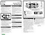
Illustration: CD-C421H

SHARP CORPORATION

CP-C421H and SURROUND
(GBOXS00018AWZZ)Constitute CD-C421H.

• In the interests of user-safety the set should be restored to its

original condition and only parts identical to those specified be
used.

Illustration: CD-C411H

CD-C421H

CD-C411H

CP-C411H Constitute CD-C411H.

This document has been published to be used
for after sales service only.
The contents are subject to change without notice.

Summary of Contents for CD-C411H

Page 1: ...D CHANGER CONTROL CD SECTION 38 FUNCTION TABLE OF IC 42 FL DISPLAY 50 REPLACEMENT PARTS LIST EXPLODED VIEW PACKING OF THE SET For U K Only Illustration CD C421H SHARP CORPORATION CP C421H and SURROUND GBOXS00018AWZZ Constitute CD C421H In the interests of user safety the set should be restored to its original condition and only parts identical to those specified be used Illustration CD C411H CD C4...

Page 2: ...ISUUSLUOKAN 1 YLITTÄVÄLLE NÄKYMÄTTÖMÄLLE LASERSÄTEILYLLE VARNING OM APPARATEN ANVÄNDS PÅANNAT SÄTTÄN I DENNA BRUKSANVISNING SPECIFICERAS KANANVÄNDAREN UTSÄTTAS FÖR OSYNLIG LASERSTRÅLNING SOM ÖVERSKRIDER GRÄNSEN FÖR LASERKLASS 1 Before returning the unit to the customer after completion of a repair or adjustment it is necessary for the following withstand voltage test to be applied to ensure the un...

Page 3: ...nce 5 4 ohms Dimensions Width 180 mm 7 1 8 Height 300 mm 11 13 16 Depth 204 mm 8 1 16 Weight 2 1 kg 4 6 lbs each Surround speaker section Type 10 cm 4 full range speaker Maximum input power 10 W Impedance 16 ohms Dimensions Width 170 mm 6 11 16 Height 120 mm 4 3 4 Depth 175 mm 6 7 8 Weight 0 6 kg 1 3 lbs each General Power source AC 230 V 50 Hz Power consumption 32 W Dimensions Width 270 mm 10 5 8...

Page 4: ...formation Search Button 26 EON Button 27 Memory Set Button 28 Record Pause Button 29 Extra Bass Equalizer Mode Button 30 Function Selector Buttons 31 ASPM Button 32 Display Mode Selector Button 33 Clock Button 34 Timer Sleep Button 35 CD Track Down Review Button TUNER Preset Down button 36 Stop Button 37 Play Repeat Button 38 CD Track Up Cue Button TUNER Preset Up button 39 Random Demo Button 40 V...

Page 5: ... Tuner control section 12 Programme Type Traffic Information Search Button 13 Preset Up Down Buttons Tape control section 14 TAPE 1 2 Stop Button 15 TAPE 1 Play Button 16 TAPE 2 Record Pause Button 17 TAPE 2 Play Button 18 TAPE 2 Rewind Button 19 TAPE 2 Fast Forward Button 20 Function Selector Buttons 21 Extra Bass Equalizer Mode Button 22 Onn Stand by Button 23 Volume Up Down Buttons CD C421H C41...

Page 6: ...sconnected the clock display will go out When the AC power supply is restored the clock display will flash on and off to indicate the time when the power failure occurred or when the AC power lead was disconnected ON STAND BY CLOCK MEMORY SET TUNING TIME AM 0 00 AM 12 00 0 00 2 3 4 7 6 5 8 9 If this happens follow the procedure below to change the clock time To change the clock time When the unit ...

Page 7: ...et C3 x4 4 Back Board 1 Screw D1 x6 7 2 5 Tuner PWB 1 Screw E1 x3 8 1 2 Socket E2 x1 6 Switch PWB 1 Screw F1 x6 8 1 2 Display PWB 2 Screw F2 x2 Main PWB 3 Socket F3 x4 7 Front Panel 1 Screw G1 x3 8 2 2 Hook G2 x2 8 Tape Mechanism 1 Open the cassette holder 8 2 2 Screw H1 x6 9 Turntable 1 Screw J1 x1 8 3 2 Cover J2 x1 10 Disc Tray 1 Screw K1 x2 8 3 2 Guide K2 x2 11 CD Changer 1 Screw L1 x4 8 4 Mech...

Page 8: ...F1 x1 ø3 x 8mm F2 x1 ø3 x10mm F1 x3 ø3 x10mm F2 x1 ø3 x10mm E1 x3 ø3 x10mm F1 x2 ø3 x10mm Main PWB Tuner PWB Display PWB Switch PWB Front Panel F3 x1 G1 x3 ø3x10mm H1 x6 ø3x10mm G2 x1 G2 x1 Tape Mechanism Cassette Holder Front Panel Power PWB Open K1 x1 ø2 x 4mm K1 x1 ø2 x 4mm J1 x1 ø3 x10mm Turntable Disc Tray J2 x1 K2 x1 K2 x1 CD Player Unit Washer L1 x4 ø2 6 x 5mm M1 x1 ø2 6 x10mm CD Changer Me...

Page 9: ...1 Remove the screws B1 x 2 pcs to remove the shaft B2 x 1 pcs 2 Remove the stop washer B3 x 1 pc to remove the gear B4 x 1 pc 3 Remove the pickup REMOVING AND REINSTALLING THE MAIN PARTS CD MECHANISM SECTION Perform steps 1 2 3 13 and 14 of the disassembly method to remove the CD mechanism How to remove the loading motor See Fig 9 3 1 Remove the screws A1 x 2 pcs to remove the loading motor A1 x2 ...

Page 10: ...parts in the FM front end section are prepared in a complete unit so you can t obtain each part individually Adjusting Parts Instrument Connection Frequency Display Frequency FM Mute Level Signal generator 1 kHz 40 kHz dev FM modulated 98 00 MHz 98 00 MHz VR351 Input Antenna 25 dBµV Output Speaker Terminal MECHANISM SECTION Driving Force Check Torque Meter Specified Value Play TW 2412 Tape 1 Over ...

Page 11: ...e optimal settings CD SECTION Figure 11 1 Note Only in STOP state it is possible to slide the pickup with the or key VOL Last memory BAL CENTER R GEQ FLAT X BAS OFF Canceling method POWER OFF Setting the test mode Any one of test mode can be set by pressing several keys as follows REC PAUSE CD POWER TEST CD operation test TEST mode Function CD test mode Setting of TEST mode Indication of CD TST mo...

Page 12: ...5 Information Provided by RDS With the CD C421 C411H you can display two types of RDS service To show them in the display press the DISPLAY MODE button Each time you press the DISPLAY MODE button the display will change to show the following information PS Programme Service Station names commonly known will be diaplayed NO PS appears if no signal is being sent PTY Progamme Type Programme type will...

Page 13: ...e with same format ASPM operation untill 108 MHz After reached 108 MHz displayed the TTL quantity of memorized stations And return to the previous receiving freq automatically Displayed the TTL quantity of memo rized stations by ASPM operation on this time And return to the previous receiving freq automatically Yes No Yes Yes Yes Yes No No No No No No Effect Pass No effect Pass No effect Pass No e...

Page 14: ...ation ASPM Comparing field strength only one strongest RDS station is memorized of all stations repeater relay stations that have same PI code Same PI code freq different AF S PS same PTY same Each PI has AF S list by individually Exa P1 has f1 f2 f3 same PTY P2 has f4 f5 same PTY For example Pickup and memorized to preset CH f 1 f 2 f 3 P 1 PI cord PS 1 Station Name f 5 f 4 P 2 PS 2 f 6 f 7 f 8 P...

Page 15: ...itch TN ON station When ON station is NO RDS NO signal TA OFF or different PTY items The receiver switch back ON TN displaying NO READY 13 During receive ON station when ON station become to be NO RDS NO signal TA ON to OFF or different PTY item The receiver switch back ON TN 14 EON TI PTY Switch TN ON in case of 2 more stations exist comparing field strength and switch to the strongest station if...

Page 16: ...tate 4 In the power section a tape is being played back 5 In the CD section the CD is stopped Parts marked with are important for maintaining the safety of the set Be sure to replace these parts with specified ones for maintaining the safety and performance of the set NOTES ON SCHEMATIC DIAGRAM Resistor To differentiate the units of resistors such symbol as K and M are used the symbol K means 1000...

Page 17: ...VO AMP 6 1 9 5 B1 B1 12V 5V TO IC401 RES CQCK COIN SQOUT RWC WRQ CL DAT SELIAL CONTROL CE Q93 Q91 SL SL DRF 7 3 9 8 7 6 5 4 3 2 1 GND D MECHA UP GND D DISK NO OPEN CLOSE GND D M M GND M SOL 9 8 7 6 5 4 3 2 1 CNP10 M 62 64 56 55 45 36 23 43 37 38 39 40 24 25 10 10 26 58 53 10 12 20 32 40 43 44 53 52 51 54 31 30 29 23 27 16 15 41 44 Q1 TO MAIN SECTION IC91 TA7291 LODING MOTOR DRIVER XOUT EFMO EFMIN ...

Page 18: ...E CL DI CF301 FM FRONT END FE301 Q360 Q371 Q602 Q601 MUTING MPX VCO CUT R L Q353 Q354 MPX IN FM AM OUT IF IN SD FM MONO ST MONO ST AM RF IN AFC IN OUT VR351 FM MUTE LEVEL AM OSC REG IN OUT VCC FM IF IN AMP FM IF Q301 FM IF FM OSC STEREO AM IN FM IN FMOSC T351 AM IF GND OSC FM FM IF AM RF SWM4 F A S SWM3 FOOL PROOF SWM5 MM1 TAPE MOTOR M SOLM1 B5 SOLENOID PHM1 CAM L SO401 AUX IN CNP303 R R L CH R CH...

Page 19: ...701 FL701 IC601 IX0225AW MAIN SYSTEM MICROCOMPUTER B2 POWER REC MUTE REC P B TA MOT SW TA SOL T1 T2 BIAS 13 4 3 11 MUTE L R R L OUT R OUT 9 2 5 12 R IN L IN 7 VCC 14 NF 8 12V DRIVER 12V AUDIO B5 B4 OUT L R IC961 LA4550 421H LA4551 411H POWER AMP B4 VDD X BASS VSS VREF LVREF RVREF AVSS GRAPHIC EQUALIZER VOLUME 58 55 R R L L L APE IDEO UNER D VOLTAGE REGULATOR VOLTAGE REGULATOR VOLTAGE REGULATOR B2 ...

Page 20: ... 0 5ms 5 0 V HFL 0 5ms 5 0 V TES REVIEW 50ms 10 0 V JP CUE 50ms 10 0 V JP 50ms 0 50 V JP 50ms 1 00 V TE 0 5ms 10 0 V JP 0 5ms 10 0 V JP 0 5ms 0 50 V JP 0 5ms 1 00 V TE REVIEW 50ms 10 0 V JP 50ms 10 0 V JP 50ms 0 50 V JP 50ms 1 00 V TE 0 5ms 10 0 V JP 0 5ms 10 0 V JP 0 5ms 0 50 V JP 0 5ms 1 00 V TE PLAY 20ms 1 00 V SPO NORMAL DISC TN0 01 20ms 2 00 V CLV PLAY TCD 712 140mm TN0 01 50ms 1 00 V SPO 50m...

Page 21: ... SW720 TUNING DOWN TIME ZD701 RX701 D703 D702 D701 FW703 C719 C718 C717 C715 R789 SW714 VOLUME UP SW722 X BASS EQUALIZER SW721 VOLUME DOWN SW712 REC PAUSE SW718 FF PRESET UP SW713 TUNING UP TIME SW715 RANDOM DEMO 41 40 37 36 35 34 33 32 31 30 29 28 27 26 25 24 23 22 21 20 19 18 17 16 15 14 13 12 11 10 9 8 7 6 5 2 1 FW702 9 1 CNS702 9 1 CNS701 1 5 10 15 20 24 25 30 35 40 41 45 50 55 60 64 65 70 75 ...

Page 22: ...E C B 1 2 3 1 2 3 E C B E C B E C B Q511 Q514 Q512 Q513 CNS703 Q565 Q583 Q582 Q581 C583 C581 Q584 Q566 D941 L942 C557 R981 L963 R982 CNS902 FW902 C975 1 1 1 2 3 1 2 3 4 5 6 7 2 3 FW703 1 9 JK961 HEADPHONES HEADPHONE PWB A4 SO961 SPEAKER TERMINAL FRONT SPEAKERS 421H 5 4 OHMS MIN 411H 8 OHMS MIN RIGHT LEFT RIGHT LEFT REAR SPEAKERS 16 OHMS MIN CNS501 CNS502 TO TAPE MECHANISUM TAPE1 HEAD P24 4 H CNS90...

Page 23: ...0 TO CD MECHANISM P25 8 E TO CD MECHANISM P25 8 C TO CD MECHANISM P25 8 G TO CD MECHANISM P25 8 C CNS2A CNS3A CNS1A CNS303 TO TUNER PWB P26 8 C IC5 IC2 IC1 IC401 IC601 R2 R3 R4 R5 R11 R7 R28 R19 C15 C12 R17 C14 R16 R15 R14 R13 R12 R9 C10 R8 C411 R413 R415 C417 R417 C4 R6 R43 R42 R25 R24 R21 R23 R22 C16 R20 C25 R40 R10 R95 R88 R31 R30 C20 C95 R96 R98 1 2 3 4 5 6 7 8 9 R97 C31 R35 R37 R32 R33 C30 C5...

Page 24: ...07 C909 D908 D906 C905 C906 D910 C904 D905 D907 C910 R901 D911 D909 C902 Q901 ZD901 B C E C901 R903 R907 R906 CNSM1 TO MAIN PWB P22 2 A CNP901 TO MAIN PWB P22 3 F MM1 TAPE MOTOR 203 7 WH BK SOLM1 SOLENOID 203 8 SWM5 CAM BK WH TAPE MECHANISM PWB D POWER PWB B WH PK BK TAPE 1 PLAYBACK HEAD 203 6 TAPE 2 ERASE HEAD 203 5 RECORD PLAYBACK HEAD 203 6 YL WH BL PK WH BK GY GY GY BL CNS502 CNS501 YL WH BK P...

Page 25: ...W2 MECHA UP SW1 OPEN CLOSE M3 T T UP DOWN LOADING SW3 DISC NUMBER CNS1B CNS1A CNS2B CNS2A CNS3B CNS3A BL YL PK WH BK GY RD WH GY WH GY WH GY WH RD WH GY WH GY WH BL PK WH YL BK 1 2 3 4 5 6 7 8 1 2 3 4 5 6 7 8 1 2 3 4 5 6 1 2 3 4 5 6 1 2 3 4 5 1 2 3 4 5 PICKUP UNIT 306 CD MOTOR PWB F SENSOR PWB E SOLM2 SOLENOID CNP1 TO MAIN PWB P23 12 E CNP2 TO MAIN PWB P23 12 C CNP10 TO MAIN PWB P23 12 B CNP3 TO M...

Page 26: ...51 C399 C398 C358 C357 R353 C356 R359 R367 RT49 R354 LT22 12 11 10 9 8 7 6 5 4 3 2 1 RT48 RT37 RT36 RT35 RT28 RT30 CT29 CT22 1 5 10 12 13 15 20 24 CT25 CT24 CT37 R366 R365 R370 RT21 RT29 ICT21 RT26 CT28 CT27 CT26 XT21 R377 D353 R368 C375 CNS303 C370 ZDT351 C396 CF352 R392 L352 R391 R395 Q361 ZD352 C391 VR351 D352 D351 R382 Q360 Q371 FE301 CNP301 2 1 L341 Q301 T302 CF301 T306 VD301 2 CF302 L354 Q35...

Page 27: ...2 PIN NO VOLTAGE IC303 0 4V 11 3V 0V 0V 1 2V 1 2V 0V 0V 0V 0V 4 6V 4 6V 4 5V 4 5V 0V 0V 0V 0V 1 1V 0V 5 5V 5 5V 0V 0V 9 8 7 6 5 4 3 2 1 12 11 10 0V 2 6V 0 5V 0 1V 0V 0V 1 5V 0V 5 6V 5 3V 1 2V 1V 1 2V 1V 3 8V 1 2V 17 16 15 14 13 20 19 18 0V 0V 2 8V 2 6V 21 22 PIN NO VOLTAGE IC302 5V 0 3V 0V 0V 1V 0V 1 7V 0V 5 6V 0 4V 1 7V 0V 5 7V 0 4V 5 6V 0 3V 5 7V 0 3V 9 8 7 6 5 4 3 2 1 PIN NO VOLTAGE IC301 0V 1 ...

Page 28: ...MAIN_STB POWER_CONT PUIN GND DSP_RES SL SL CQCK COIN SQOUT WRQ RWC MAIN_STB CLEAR MAIN_SI MAIN_SO MAIN_SCK MAIN_SI MAIN_SO MAIN_SCK CLEAR 5 6V REC P B REC MUTE CD DRF CD PUIN CD SL CD SL CD RES CD SQOUT CD COIN CD CQCK VDD CD RWC CD WRQ TACUM SW T2 RUN T1 RUN TA MOT SW TA SOL VSS U D SW D NO SW O C SW VDD POWER_CONT VLOAD P33 P12 P10 AVDD AVREF P04 XT1 P74 P73 AVSS RESET P26 P25 P24 P23 P126 X1 P1...

Page 29: ...1 50 R563 470 C520 330P R520 1K C504 330P R584 10K R510 10K Q575 KTC3199 GR Q583 KRC104 M C581 0 047 R502 1K R566 4 7K R555 560 C533 0 018 C537 0 015 C535 560P C564 22 16 R541 22K Q512 2SC1845 F R558 56 C558 0 068 Q581 KTA1266 GR IC501 AN7345K PLAYBACK AND RECORD PLAYBACK AMP R538 5 6K R581 10K R536 56 Q514 2SC1845 F R501 1K R582 10K R583 10K Q515 KTC3199 GR Q566 KTA1266 GR R542 68K R570 47K R577 ...

Page 30: ...1 2 3 4 5 6 21 22 23 20 5 4 1 2 3 5 4 3 2 1 5 4 3 2 1 1 2 3 4 5 6 7 8 9 10 11 12 13 14 15 16 17 18 19 20 21 22 23 24 25 26 27 28 29 30 31 32 33 34 35 36 1 2 3 4 5 6 7 8 9 10 11 12 13 14 15 16 17 18 19 20 21 22 23 24 25 26 27 28 29 30 31 32 33 34 35 36 37 38 39 40 41 42 43 44 45 46 47 48 49 50 51 52 53 54 55 56 57 58 59 60 61 62 63 64 M2 SLED MOTOR M1 DISC MOTOR CNS1B CNS1A C25 0 01 HF CV CV SLOF H...

Page 31: ...CLOSE BIM5 CNS10 XL1 16 93MHz C50 0 1 C59 0 022 C51 0 022 CS TEST5 X TAL GENERATOR 4M 16M RES CQCK COIN SQOUT RWC WRQ FSX PW SFSY SBCK TEST11 U COM INTERFACE SUB CODE EFLG SBSY XVSS XIN XOUT XVDD MUTER RVDD RCHO RVSS LVSS LCHO LVDD MUTEL TEST4 TEST1 4FS DIGITAL FILTER DOUT TEST3 DIGITAL OUT RAM ERROR COERECT FLAG CONTROL VCO CLOCK OSC CONTROL SLICE LEVEL CONTROL SYNC DETECT EFM DEMODULATE EXTERNAL...

Page 32: ...OR R962 33K C944 0 1 ML C962 0 0015 IC961 LA4451 411H LA4450 421H POWER AMP C949 2200 50 R941 10K R944 1 1 2 C941 0 022 C968 0 001 C972 0 001 R966 1K 8 9 5 6 7 11 10 6 7 8 9 5 4 1 2 3 4 5 6 7 3 2 1 1 2 3 4 5 6 7 1 2 3 4 5 6 7 8 9 10 11 12 13 14 1 3 1 3 2 2 D941 1SS133 D943 1SS133 D942 1SS133 12V 12V VP VF2 VF1 5V 12V POWER 5V UCOM 5V SERVO MECHA MAIN_L MAIN_R GND A_GND DRIVER AUDIO CHASSIS GND D L...

Page 33: ... 0 022 C924 0 0012 411H 0 001 421H C923 0 0012 411H 0 001 421H C925 0 0033 C926 0 0033 C983 0 047 ML C922 0 022 D907 RL104A D901 D901 D904 RL203F 411H 1N5402M 422H R901 220 C902 47 50 R903 220 R905 3 3K R904 100 ZD902 MTZJ30B C907 2 2 C904 47 50 R906 2 2 Q901 KTA1266 GR C905 100 50 C910 0 047 ML C949 2200 50 JK961 HEADPHONES D909 RL104A 1 2 3 4 5 6 7 1 2 3 4 5 6 7 1 2 3 4 5 6 7 FW902 PT901 POWER T...

Page 34: ...7 S18 S19 S20 S21 VDD VSS REMOCON SYS STOP POWER AR_P IC P01 INTP1 P02 INTP2 P03 INTP3 CI0 P71 P72 P70 P00 INTP0 TI0 P16 ANI6 P17 ANI7 AVSS P74 RESET P24 BUSY P25 SI0 SB0 P27 SCK0 P23 STB P22 SCK1 P21 SO1 P20 SI1 P90 FIP2 P80 FIP0 P81 FIP1 P91 FIP3 P92 FIP4 P93 FIP5 P94 FIP6 P113 FIP21 P114 FIP22 P115 FIP23 P127 FIP33 P116 FIP24 P117 FIP25 P120 FIP26 P121 FIP27 P122 FIP28 P123 FIP29 P124 FIP30 P12...

Page 35: ... TO0 X1 X2 VSS AVREF AVDD KEY 0 KEY 1 KEY 2 KEY 3 XT2 P04 5V BACK UP 1 2 3 4 5 6 7 8 R701 10K SW726 SW725 R759 12K R760 12K FW701 R752 10K R751 1K R754 10K SW722 SW721 R741 3 9K SW716 R744 2 2K SW714 D703 1SS133 C713 0 01 D705 1SS133 R793 100K L701 100µH R765 10K 1K R766 1K TER R750 1K R749 1K R748 1K SW701 SW706 SW715 SW713 R738 33K SW705 SW718 SW717 R745 3 9K R703 1 2K R711 2 2K R731 12K R708 1K...

Page 36: ...380 10 16 R378 82K R373 1K R372 1K R374 1K R371 1K C350 0 022 C352 10 16 C351 0 022 R351 5 6K C353 0 022 C354 0 022 R393 1K C364 10 16 C366 0 001 C365 0 022 C363 0 022 C343 33P VR351 10K B D301 1SS133 CNP301 R349 33 R344 470 R345 4 7K R301 330 C346 0 022 C345 0 022 C321 100 16 R379 2 2K C382 15P C381 12P X352 4 5MHz C385 0 01 R377 47K L351 100µH R358 8 2K C342 0 022 IC30 LA18 CF351 C361 0 022 D304...

Page 37: ...1SS133 R376 1K R378 82K C386 330P CNS303 R373 1K R354 3 9K C399 0 022 C353 0 022 C354 0 022 R393 1K C358 1 50 ZDT351 MTZJ5 1B RT49 390 RT48 390 CT43 10 16 RT21 100K RT26 1K RT28 1K RT30 1K LT22 2 2µH RT37 220K RT36 220K C366 0 001 C365 0 022 R356 1K C369 27P C373 0 033 C374 0 033 R357 470K R364 1 5K C385 0 01 R377 47K L351 100µH R363 1 5K R366 10K R368 33K R365 10K C375 3 3 50 R367 1K Q353 KTC3199...

Page 38: ... stop Is from 5 V till 2 5V down pulse approx 300 ms Check the SWM3 and the wiring from the IC701 pin 21 to the SWM3 No No input into the IC701 pin 21 when the turntable is rotating 5V 2 5V 0V Yes Check IC2 pin26 Q91 and Q93 and the periphery Check the MECHA UP SW and the wiring from the IC701 pin 21 to the MECHA UP SW No Yes Is there following voltage input on the IC701 pin 21 in the specific sta...

Page 39: ...2 pins 24 and 25 IC91 pins 1 and 3 The CD function will not work The CD operating keys don t work Check the CD DSP power supply and 16 93 MHz clock and reset terminal Check the waveform of SCK SO DATA and SI COMM Yes Yes See if the pick up is in the PICKUP IN SW position If the items mentioned above are OK check the main microcomputer IC701 Yes Yes No Yes No The CD operating keys work Check the Fo...

Page 40: ...Figure 40 2 Figure 40 1 Waveform in case of normal play back HF 1 0V DIV 0 5µsec DIV DC When playing back the disc 3 2 1 4 0 5s 1 00 V IC1 16 FD 0 5s 10 0 V IC2 13 CLV 0 5s 10 0 V IC1 54 DRF 0 5s 2 00 V IC1 7 TE Check the tracking system Check waveform of IC1 pin 7 TE Play is possible in TEST mode Although IL is possible play is impossible Check the periphery of IC 1 pin 14 Normal jump is impeded ...

Page 41: ... is performed when disc exits Yes Although HF waveform is normal TOC data cannot be read Yes Check PDO waveform Fig 41 Abnormal Check the IC1 pins 43 and 44 IC2 pins 3 5 7 10 and 11 Stop Play As VCO freque ncy is locked at 4 32 M Hz voltage of PDO rises and stabili zes 2 3 0 5s 1 00 V IC2 3 PDO 0 5s 1 00 V IC2 16 FD Although HF waveform is normal and the time indication is normal no sound is emitt...

Page 42: ...D Power terminal of digital system 24 CONT1 Input Output General purpose input output terminal 1 25 CONT2 Input Output General purpose input output terminal 2 26 CONT3 Input Output General purpose input output terminal 3 27 CONT4 Input Output General purpose input output terminal 4 28 CONT5 Input Output General purpose input output terminal 5 29 EMPH Output Difference monitor terminal At H deempha...

Page 43: ...ST5 Input Input terminal for test Pull down resistor is integrated Surely connected to 0V 63 CS Input Chip selection input terminal Pull down resistor is integrated Connected to 0when not controlled 64 TEST1 Input Input terminal for test Pull down resistor is integrated Surely connected to 0V Pin No Note The same potential must be supplied to the power terminals VDD VVDD LVDD RVDD XVDD In this uni...

Page 44: ...ndle amplifier input 25 SPG Pin to connect gain setting resistor in the 12cm mode of spindle 26 SP Pin to connect spindle phase compensation constant together with SPD pin 27 SPO Spindle control signal output pin 28 SLEO Pin to connect thread phase compensation constant 29 SLD Thread control signal output pin 30 SL Input pin of thread feed signal from micro computer 31 SL Input pin of thread feed ...

Page 45: ... Pin to connect capacitor for peak hold of RF signal 61 BHI Pin to connect capacitor for bottom hold of RF signal 62 LDD APC circuit output pin 63 LDS APC circuit output pin 64 VCC1 RF system VCC pin Figure 45 BLOCK DIAGRAM OF IC 1 FIN2 FIN1 E F TB TE TE TESI SCI TH TA TD TD JP TO FD FD FA FA FE FE AGND SP SPI SPG SP SPD SLEQ SLD SL SL JP JP TGL TOFF TES HFL SLOF CV CV RFSM RFS SLC SLI DGND FSC TB...

Page 46: ...OPEN 29 AVDD AVDD Analog VDD 30 AVREF AVREF Analog Ref Potential 31 P04 CAM SW Input TAPE CAM SW 32 XT2 Output Not used OPEN 33 VSS VSS GND Potential 34 X1 X1 Input Main Clock 4 19MHz 35 X2 X2 Output Main Clock 4 19MHz 36 P37 LMUTE Output LINE MUTE 37 38 P36 35 Output Not used OUT H OPEN 39 P34 SMUTE Output System Mute 40 P33 Output Not used OUT H OPEN 41 43 P32 30 Output Not used OUT L OPEN 44 P0...

Page 47: ...al with asterisk mark is open terminal which is not connected to the outside Function IC601 IX0225AW µPD78043 MAIN_ST AVSS MAIN SI MAIN SO MAIN SCK RESET T_RECPLY REC MUTE CRO2 FRF PUIN SW SLM1 SLM2 CD MUTE CD DSPRES CD SQIN CD COOUT CD CQCK VDD RWC WRQ AVDD AVREF CAM SW VSS X1 X2 LMUTE SMUTE T2 RUN T1 FAS T_MOTOR T_SOL IC VDD T1CRO2 SPN_P SRS_P STANBY SPRLY T2CRO2 SP_DET VSS P33 ANI2 ANI0 AVDD AV...

Page 48: ...EF A D Converter Reference Input 31 XT1 VSS Input Sub clock Input Connect with VSS 32 XT2 N C Output Sub clock Output OPEN 33 VSS VSS Connect with GND 34 X1 X1 Input Main Clock 4 19MHz 35 X2 X2 Output Main Clock 4 19NHz 36 P37 LED LCK Output LED IC Serial Clock Output BU2092 LCK 37 P36 LED DATA Output LED IC Serial Data Output BU2092 Data 38 P35 LED CLK Output LED IC Serial Clock Output BU2092 CLK...

Page 49: ...2 ANI2 P13 ANI3 P16 ANI6 P15 ANI5 P14 ANI4 P17 ANI7 AVSS P74 RESET P24 BUSY P25 SI0 SB0 P27 SCK0 P23 STB P22 SCK1 P21 SO1 P20 SI1 P90 FIP2 P80 FIP0 P81 FIP1 P91 FIP3 P92 FIP4 P93 FIP5 P94 FIP6 P113 FIP21 P114 FIP22 P115 FIP23 P127 FIP33 P116 FIP24 P117 FIP25 P120 FIP26 P121 FIP27 P122 FIP28 P123 FIP29 P124 FIP30 P125 FIP31 P126 FIP32 VLOAD P97 FIP9 P96 FIP8 P95 FIP7 P105 FIP15 P104 FIP14 P102 FIP1...

Page 50: ...Gain2 NC Vcc Reg5V OP1 Vref out TSD Stand by Gain4 VM4 Pre driver Pre driver VM4 Gain1 5K 15K 15K 2K 23K 23K 5K 10K 10K 10K 10K VM1 VM1 OP1 PA PA OP1 PA PA VM3 Vctl3 out Vctl3 Vctl3 Vcc Vcc Vcc GND GND GND GND GND GND GND GND GND Regbase Reg5V Pre driver Pre driver VM3 Gain2 NC 5K 1 23V 10K 10K 10K 10K 10K VM2 VM2 OP1 OP1 PA PA OP1 PA PA Standby SS GND Standby Gain4 Vctl4 VM4 VM4 VM3 VM3 Vctl3 out...

Page 51: ...Gain2 NC Vcc Reg5V OP1 Vref out TSD Stand by Gain4 VM4 Pre driver Pre driver VM4 Gain1 5K 15K 15K 2K 23K 23K 5K 10K 10K 10K 10K VM1 VM1 OP1 PA PA OP1 PA PA VM3 Vctl3 out Vctl3 Vctl3 Vcc Vcc Vcc GND GND GND GND GND GND GND GND GND Regbase Reg5V Pre driver Pre driver VM3 Gain2 NC 5K 1 23V 10K 10K 10K 10K 10K VM2 VM2 OP1 OP1 PA PA OP1 PA PA Standby SS GND Standby Gain4 Vctl4 VM4 VM4 VM3 VM3 Vctl3 out...

Reviews: