background image

SHARP CORPORATION

This document has been published to be used for after
sales service only.
The contents are subject to change without notice.

In the interests of user-safety (Required by safety regulations in some countries ) the set should be restored to its
original condition and only parts identical to those specified should be used.

Page

»

 ELECTRICAL SPECIFICATIONS ......................................................................................................... 1

»

 IMPORTANT SERVICE SAFETY PRECAUTION ................................................................................. 2

»

 LOCATION OF USER'S CONTROL ..................................................................................................... 4

»

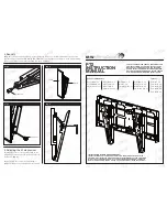
 INSTALLATION AND SERVICE INSTRUCTIONS ................................................................................ 5

»

 SERVICE ADJUSTMENT ..................................................................................................................... 9

»

 CHASSIS LAYOUT ............................................................................................................................. 12

»

 BLOCK DIAGRAM .............................................................................................................................. 13

»

 DESCRIPTION OF SCHEMATIC DIAGRAM

S

 & WAVEFORMS ............

.

...........................................14

»

 SCHEMATIC DIAGRAMS ................................................................................................................... 15

»

 PRINTED WIRING BOARD ASSEMBLIES ........................................................................................ 22

»

 PARTS LIST ........................................................................................................................................ 27

»

 PACKING OF THE SET ...................................................................................................................... 3

6

CONTENTS

SPEAKER

SIZE ..........................................................

12

 x 5 cm oval (2 pcs.)

VOICE COIL IMPEDANCE ............................ 16 ohm at 400 Hz

ANTENNA INPUT IMPEDANCE

VHF/UHF ..................................................... 75 ohm Unbalanced

TUNING RANGES

VHF-Channels ............................................................... 2 thru 13

UHF-Channels ............................................................ 14 thru 69

CATV Channels ........................................................... 1 thru 125

POWER INPUT ..................................................... 120V AC, 60 Hz

POWER RATING ................................................................... 1

55

W

PICTURE SIZE ..........................................

3

,

073

 cm

(

476

sq inch)

CONVERGENCE ............................................................. Magnetic

SWEEP DEFLECTION .................................................... Magnetic

FOCUS ............................................... Hi-Bi-Potential Electrostatic

INTERMEDIATE FREQUENCIES

Picture IF Carrier Frequency ...... 45.75 MHz (Analog Terrestrial)
Sound IF Carrier Frequency....... 41.25 MHz (Analog Terrestrial)
Color Sub-Carrier Frequency ..... 42.17 MHz (Analog Terrestrial)

 (Nominal)

AUDIO POWER

OUTPUT RATING .............. 3.0W + 3.0W (at 10% distortion and

Dual CH Operate)

Specifications are subject to change without
prior notice.

ELECTRICAL SPECIFICATIONS

MODEL

SERVICE MANUAL

32SC260

COLOR TELEVISION

Digital Terrestrial Broadcast (VHF/UHF) .......................2 thru 69

Chassis No. 

GB-3D(1W)

IF Center Frequency ........................ 44 MHz (Digital Terrestrial)

(EIA, Channel Plan U.S.A.)

32

SC260

Summary of Contents for 32SC260

Page 1: ...cm oval 2 pcs VOICE COIL IMPEDANCE 16 ohm at 400 Hz ANTENNA INPUT IMPEDANCE VHF UHF 75 ohm Unbalanced TUNING RANGES VHF Channels 2 thru 13 UHF Channels 14 thru 69 CATV Channels 1 thru 125 POWER INPUT 120V AC 60 Hz POWER RATING 155W PICTURE SIZE 3 073 cm2 476sq inch CONVERGENCE Magnetic SWEEP DEFLECTION Magnetic FOCUS Hi Bi Potential Electrostatic INTERMEDIATE FREQUENCIES Picture IF Carrier Frequen...

Page 2: ...e with a meter to be certain that the high voltage does not exceed the specified value and that it is regulating correctly 5 Do not use a picture tube other than that specified or make unrecommended circuit modifications to the high voltage circuitry 6 When trouble shooting and taking test measurements on a receiver with excessive high voltage avoid being unnecessarily close to the receiver Do not...

Page 3: ...mechanical insulators etc 3 To be sure that no shock hazard exists check for leakage current in the following manner Plug the AC cord directly into a 120 volt AC outlet Do not use an isolation transformer for this test Using two clip leads connect a 1 5k ohm 10 watt resistor paralleled by a 0 15µF capacitor in series with all exposed metal cabinet parts and a known earth ground such as electrical ...

Page 4: ...utton CHANNEL UP DOWN Selects next higher channel Selects next lower channel Moves the mark on the MENU screens Infrared Transmitter Window DISPLAY Press Displays receiving channel for 4 seconds Press again Removes display Temporarily displays receiving channel when in Closed Caption mode MENU Press Accesses MAIN MENU Press again Exits MAIN MENU Note The above shaded buttons on the Remote Control ...

Page 5: ...the horizontal oscillator does not stop in step 5 the circuit must be repaired before the set is returned to the customer HIGH VOLTAGE CHECK High voltage is not adjustable but must be checked to verify that the receiver is operating within safe and efficient design limitations as specified checks should be as follows 1 Connect an accurate high voltage meter between ground and anode of picture tube...

Page 6: ...e from V01 to M05 Select the item you wish to adjust 3 Data number selection Press the Vol up or Vol down button to adjust the data number To enter the service mode and exit serv ice mode To enter the service mode manually just press and hold the Vol down and Ch up buttons at the same time plug the AC cord into a wall socket Now the TV set is switched on and enters the service mode To exit the ser...

Page 7: ... Component Input V49 G R DRIVE COMPONENT 0 127 00h 7Fh 64 40h Component Input V50 B DRIVE COMPONENT 0 127 00h 7Fh 64 40h Component Input V51 SHARP COMPONENT 0 63 00h 3Fh 44 2Ch Component Input 2C V52 TINT S 0 127 00h 7Fh 62 3Eh S Terminal Input 3E V53 C TRAP 0 1 00h 01h 00 00h 00 V59 AUTO FRESH 0 1 00h 01h 00 00h 00 V60 SHARP P F 0 1 00h 01h 01 01h 01 V61 CD MATRIX 0 3 00h 03h 02 02h 02 V62 B Y AT...

Page 8: ...V S CORRECTION 0 15 00h 0Fh 12 0Ch 0B D07 EW PARABOLA 0 63 00h 3Fh 43 2Bh D08 EW TRAPEZIUM 0 63 00h 3Fh 36 24h D10 AFC GAIN 0 3 00h 03h 02 02h 02 D11 V EHT 0 7 00h 07h 06 06h 06 D12 H EHT 0 7 00h 07h 06 06h 06 D13 EW CORNER 0 31 00h 1Fh 08 08h 0F D14 EW CORNER BOTTOM 19 81 13h 51h 50 32h 32 D15 NOISE DET LEVEL 0 3 00h 03h 00 00h 00 D18 V CENTERING 0 63 00 3Fh 36 24h D19 V AGC 0 1 00h 01h 00 00h 00...

Page 9: ...e adjustment V03 and set to 00 minimum color Record original data code under adjustment V03 before changing V03 does not have to be adjusted if you selected a B W picture or monoscope pattern 3 Alternately adjust the service adjustment data of V09 and V10 until a good grey scale with normal whites is obtained RF Input 4 For component input the data value of V49 and V50 is adjusted to follow the da...

Page 10: ...ustment select data bus D05 and adjust to get the proper vertical linearity SCREEN FORMAT 16 9 5 Input data of D22 to mines 30 step from D03 data V SIZE 6 Input data of D24 same as D05 data V LIN Note Aging for 10 min before adjustment After the adjustment of V center and V size re adjustment for this V line Vertical Phase Adjustment SCREEN FORMAT 4 3 1 Enter the service mode and input data of 00h...

Page 11: ...paration Adjustment 1 Input SIGNAL 1 and vary the M04 bus data to get the minimun AC voltage to pin 39 of IC3001 2 Input SIGNAL 2 and vary the M05 bus data to get the minimun AC voltage to pin 39 of IC3001 SIGNAL 1 300Hz 30 modulation Lch only NR ON SIGNAL 2 3kHz 30 modulation Lch only NR ON Note SIGNAL 1 Adj for widebando SIGNAL 2 Adj for spectral Check the output of the speaker at the maximum vo...

Page 12: ...CHASSIS LAYOUT 32SC260 12 ...

Page 13: ...BLOCK DIAGRAM 32SC260 13 ...

Page 14: ...1 Photographs taken on a standard gated color bar signal the tint setting adjusted for proper color The wave shapes at the red green and blue cathodes of the picture tube depend on the tint color level and picture control 2 indicates waveform check points See chart waveforms are measured from point indicated to chassis ground WAVEFORMS å AND SHADED COMPONENTS SAFETY RELATED PARTS ç MARK X RAY RELA...

Page 15: ...6 5 4 3 2 1 A B C D E F G H SCHEMATIC DIAGRAM CRT Unit 15 32SC260 ...

Page 16: ...A B C D E F G H 10 9 8 7 6 5 4 3 2 1 SCHEMATIC DIAGRAM MAIN 1 Unit 16 32SC260 ...

Page 17: ...17 16 19 18 15 14 13 12 11 10 17 32SC260 ...

Page 18: ...A B C D E F G H 10 9 8 7 6 5 4 3 2 1 SCHEMATIC DIAGRAM MAIN 1 Unit 18 32SC260 ...

Page 19: ...17 16 19 18 15 14 13 12 11 10 19 32SC260 ...

Page 20: ...A B C D E F G H 10 9 8 7 6 5 4 3 2 1 SCHEMATIC DIAGRAM MAIN 1 Unit 20 32SC260 ...

Page 21: ...17 16 19 18 15 14 13 12 11 10 21 32SC260 ...

Page 22: ...8 7 10 9 6 5 4 3 2 1 A B C D E F G H PRINTED WIRING BOARD ASSEMBLIES PWB A MAIN Unit Wiring Components Side 32SC260 22 ...

Page 23: ...17 16 19 18 15 14 13 12 11 10 32SC260 23 ...

Page 24: ...8 7 10 9 6 5 4 3 2 1 A B C D E F G H PWB A MAIN Unit Components side 32SC260 24 ...

Page 25: ...17 16 19 18 15 14 13 12 11 10 32SC260 25 ...

Page 26: ...8 7 10 9 6 5 4 3 2 1 A B C D E F G H PWB D 2 LINE Y C Unit Wiring Side PWB B CRT Unit Wiring Side PWB D 2 LINE Y C Unit Chip Parts Side 32SC260 26 ...

Page 27: ... VHISE125N F X SE125N AF IC751 VHIPQ09RDA1 1 X PQ090RDA1SZ AE IC900 VHICXA2089Q 2Y X CXA2089Q 6T AN IC1101 VHIPQ1CZ41H 1Y X PQ1CZ41H2ZPH AG IC1102 VHIBA00BC0W 1S X BA00BC0WT V5 AF IC1103 VHINJ2584AM 1Y X NJ2584AM AH IC1104 VHIBA00BC0W 1S X BA00BC0WT V5 AF IC1403 VHIPQ05RDA1 1 X PQ050RDA1SZ AF IC2001 RH IXB644WJQ1Q X IC BA IC2040 VHIKIA7045A 1 X KIA7045AP AD IC2101 VHIBR24L16F 1Y X BR24L16F AE IC30...

Page 28: ...3 1Y X Diode AA D2060 RH EX0619GEZZY X Zener Diode 6 2V AB TH501 RH HZ0004GEZZ X Thermistor AD U VA701 RH VXA009WJZZ X VARISTOR AC U PR701 RMPTP0092CEZZ X Packaged Circuit AF X801 RCRSAA010WJZZ X Crystal AD CF302 RFILC0449CEZZ X Filter AC CF401 RFILC0446CEZZ X Filter AC CF2040 RCRM 0003CEZZ X Ceramic Vibrator AD L201 VP XF1R2K0000Y X Peaking 1 2mH AA L203 VP XF100K0000Y X Peaking 10mH AA L204 VP X...

Page 29: ... C707 RC KZ0092GEZZA X 3300p AC250V Ceramic AC Ref No Part No Description Code C723 RC EZ0724CEZZ X 100 160V EL AE C725 RC EZA065WJZZ X 330 160V EL AG C726 RC KZ0226CEZZ X 560p 2kV Ceramic AC C727 RC KZ0226CEZZ X 560p 2kV Ceramic AC C729 VCEA0A1HW106M X 10 50V EL AA C730 VCEA0A1VW108M X 1000 35V EL AD C731 RC EZ0385CEZZ X 1000 16V EL AD C732 VCKYPA2HB102K X 1000p 500V Ceramic AA C733 VCKYPA2HB102K...

Page 30: ... EL Electrolytic M Poly Metalized Polypro Film Ref No Part No Description Code C3013 VCKYCY1HB272KY X 2700p 50V Ceramic AA C3014 VCKYCY1CB473KY X 0 05 16V Ceramic AA C3015 VCEACA1HC335K X 3 3 50V EL AC C3016 VCE9GA1HW475M X 4 7 50V EL AB C3017 VCEACA1CC106K X 10 16V EL AC C3018 VCEA0A1HW105M X 1 50V EL AA C3019 VCEA0A1HW475M X 4 7 50V EL AA C3020 VCEA0A1HW475M X 4 7 50V EL AA C3021 VCEA0A1HW475M X...

Page 31: ... Ref No Part No Description Code U R624 VRS RG3DB332J X 3 3k 2W M Ox AB R625 VRD RA2BE102JY X 1k 1 8W Carbon AA R627 VRN RL3ABR47J X 0 47 1W M Film AB U R628 VRN RL3ABR47J X 0 47 1W M Film AB S U R651 VRS RG2HC270J X 27 1 2W M Ox AB S U R652 VRD RA2EE103GY X 10k 1 4W Carbon AA S U R653 VRD RA2EE562GY X 5 6k 1 4W Carbon AA R663 VRS CY1JF102JY X 1k 1 16W M Ox AA R684 VRD RA2BE472JY X 4 7k 1 8W Carbo...

Page 32: ...No Description Code R969 VRS CY1JF472FY X 4 7k 1 16W M Ox AA R970 VRD RA2BE6R8JY X 6 8 1 8W Carbon AA R971 VRS CY1JF101JY X 100 1 16W M Ox AA R972 VRS CY1JF101JY X 100 1 16W M Ox AA R973 VRS CY1JF000JY X 00 1 16W M Ox AA R974 VRS CY1JF103JY X 10k 1 16W M Ox AA R975 VRS CY1JF333JY X 33k 1 16W M Ox AA R982 VRS CY1JF750JY X 75 1 16W M Ox AA R983 VRS CY1JF473JY X 47k 1 16W M Ox AA R984 VRS CY1JF473JY ...

Page 33: ...3012 VRS CY1JF102JY X 1k 1 16W M Ox AA R3017 VRS CY1JF102JY X 1k 1 16W M Ox AA R3018 VRS CY1JF102JY X 1k 1 16W M Ox AA R3024 VRD RA2BE102JY X 1k 1 8W Carbon AA R3027 VRS CY1JF000JY X 00 1 16W M Ox AA R3029 VRS CY1JF153JY X 15k 1 16W M Ox AA R3030 VRS CY1JF473JY X 47k 1 16W M Ox AA R3031 VRS CY1JF474JY X 470k 1 16W M Ox AA RESISTORS M Ox Metal Oxide M Film Metal Film Ref No Part No Description Code...

Page 34: ... X 470 1 8W Carbon AA R876 VRD RA2BE121JY X 120 1 8W Carbon AA R877 VRD RA2BE121JY X 120 1 8W Carbon AA R878 VRD RA2BE121JY X 120 1 8W Carbon AA R879 VRD RM2HD100JY X 10 1 2W Carbon AA R880 VRC MA2HG332KY X 3 3k 1 2W Carbon AB R881 VRC MA2HG332KY X 3 3k 1 2W Carbon AB R882 VRC MA2HG332KY X 3 3k 1 2W Carbon AB R883 VRD RA2BE221JY X 220 1 8W Carbon AA R884 VRD RA2BE221JY X 220 1 8W Carbon AA R885 VR...

Page 35: ...RE DT AE J1 VW7UGB5 050KK X Lead Wire AA J3 VW7UGB4 040KK X Lead Wire AA J4 VW7UGB2 120KK X Lead Wire AB J5 VW7UGB6 060KK X Lead Wire AA J6 VW7UGB8 080KK X Lead Wire AA J7 VW7UGB4 040KK X Lead Wire AA RRMCGA450WJSA X Infrared Remote Control Unit AM TINS C218WJZZ X Operation Manual AF TGAN A216WJN1 X Guarantee Card AC RESISTORS M Ox Metal Oxide M Film Metal Film PWB D DUNTKB572WEV0 2 LINE Y C UNIT ...

Page 36: ...NG OF THE SET FRONT Packing Foam Packing Case REAR Use tape to fix the top side of packing case Use 12 staples to fix the bottom side of packing case 32SC260 Polyethylene Bag Polyethylene Mat ACCESSORIES 36 ...

Page 37: ...32SC260 37 ...

Page 38: ...echanical photocopying recording or otherwise without prior written permission of the publisher ALL RIGHTS RESERVED Design and Production Information Design base SEM Production SEMEX Modify SEMEX SHARP ELECTRONICA MEXICO S A DE C V Quality Reliability Control Center Blvd SHARP No 3510 Parque Industrial Rosarito Playas de Rosarito México B C 22710 QRC0028 U January 2006 J B ...

Reviews: