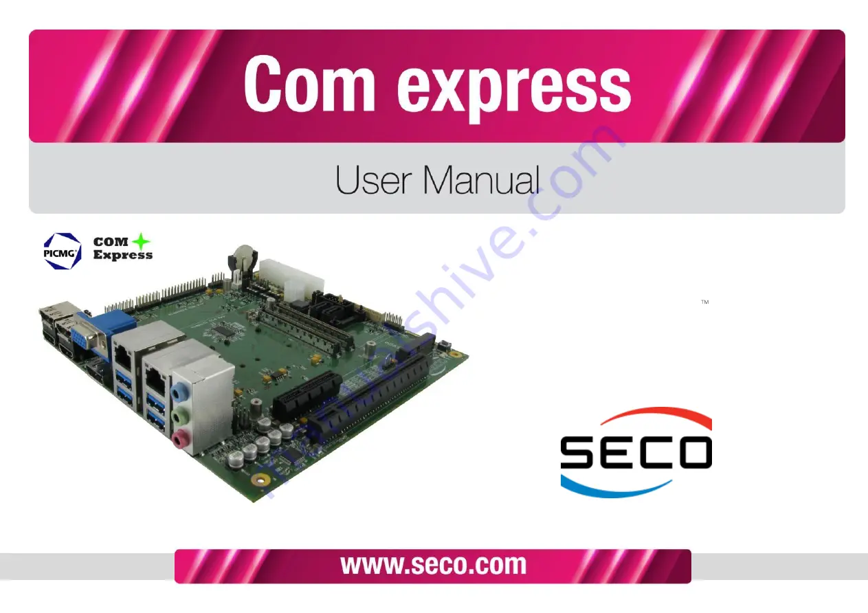
CCOMe-965
Carrier Board for COM-Express Type 6 Module
on mini-ITX form factor
Страница 1: ...CCOMe 965 Carrier Board for COM Express Type 6 Module on mini ITX form factor...
Страница 2: ...curacies errors or omissions herein SECO S r l reserves the right to change precise specifications without prior notice to supply the best product possible For further information on this module or ot...
Страница 3: ...er 2 2 1 Introduction 13 2 2 Technical Specifications 14 2 3 Electrical Specifications 15 2 3 1 RTC Battery 16 2 3 2 Power Rails meanings 16 2 4 Mechanical Specifications 17 2 5 Block Diagram 18 CONNE...
Страница 4: ...43 3 3 15 Digital Display Interface 3 Connector 45 3 3 16 PEG PCI Express Graphics x16 Connector 46 3 3 17 FAN Connector 49 3 3 18 Audio Section 50 3 3 19 I2C EEPROM socket 51 3 3 20 SPI Flash socket...
Страница 5: ...0 Last Edition 3 0 Author S B Reviewed by G G Copyright 2016 SECO S r l 5 Chapter 1 Warranty Information and assistance RMA number request Safety Electrostatic Discharges RoHS compliance Terminology a...
Страница 6: ...orisation number must be put both on the packaging and on the documents shipped with the items which must include all the accessories in their original packaging with no signs of damage to or tamperin...
Страница 7: ...s possible to send the faulty product to the SECO Repair Centre In this case follow this procedure o Returned items must be accompanied by a RMA Number Items sent without the RMA number will be not ac...
Страница 8: ...high voltages caused by static electricity could damage some or all the devices and or components on board 1 6 RoHS compliance The CCOMe 965 board is designed using RoHS compliant components and is ma...
Страница 9: ...thernet Gbps Gigabits per second GND Ground GPI O General purpose Input Output HD Audio High Definition Audio most recent standard for hardware codecs developed by Intel in 2004 for higher audio quali...
Страница 10: ...etworks SM Bus System Management Bus a subset of the I2C bus protocol dedicated to communication with devices for system management like a smart battery and other power supply related devices SPI Seri...
Страница 11: ...s high definition audio specification pdf HDMI http www hdmi org index aspx I2C http www nxp com documents other UM10204_v5 pdf Intel Front Panel I O connectivity DG http www formfactors org developer...
Страница 12: ...e 965 Rev First Edition 1 0 Last Edition 3 0 Author S B Reviewed by G G Copyright 2016 SECO S r l 12 Chapter 2 Introduction Technical Specifications Electrical Specifications Mechanical Specifications...
Страница 13: ...mance class or form factor size modules Baseboard designers can use just the I O interfaces that really need providing on the carrier board the routing to the adequate interface connectors This versat...
Страница 14: ...ne combined with SIM card slot Gen2 compatible Networking 2 x Gigabit Ethernet ports Other Interfaces I2C EEPROM Socket LPC Bus internal pin header Front Panel Header 1 x 28 pin connector for addition...
Страница 15: ...ected directly to Ground Selection of AT or ATX mode is made using jumper JP9 which is a standard pin header P2 54mm 1x3 pin The board has also an auxiliary Power Connector for 12V_S Voltages This con...
Страница 16: ...e batteries should only be replaced with devices of the same type Always check the orientation before inserting and make sure that they are aligned correctly and are not damaged or leaking Never allow...
Страница 17: ...ations According to miniITX form factor board dimensions are 170 x 170 mm 6 69 x 6 69 The printed circuit of the board is made of six layers some of them are ground planes for disturbance rejection In...
Страница 18: ...Switch LED panel header VGA connector eDP connector LVDS connector PCI Express Graphics PEG x16 Slot DP HDMI combo connector 1 DP HDMI combo connector 2 DP connector 3 COM Express A B connector SIM Sl...
Страница 19: ...CCOMe 965 CCOMe 965 Rev First Edition 1 0 Last Edition 3 0 Author S B Reviewed by G G Copyright 2016 SECO S r l 19 Chapter 3 Connectors placement Connectors overview Connectors description...
Страница 20: ...lowing picture it is possible to see the position of each connector TOP SIDE BOTTOM SIDE FAN connector PCI e x4 slot ATX power connector GPIO SD UART header Auxiliary Power SPI Flash holder Power butt...
Страница 21: ...GbEthernet 0 CN31 I2C EEPROM Socket CN13 USB 3 0 ports 2 3 GbEthernet 1 CN32 Digital Display interface 3 CN14 HD Audio Jacks CN33 Battery Holder CN15 S P DIF Out connector CN34 Switch LED Header CN16...
Страница 22: ...000Mb s link ind GBE0_LINK1000 A5 B5 LPC_AD1 LPC Address Data Bus 1 GbEthernet differential pair 2 GBE0_MDI2 A6 B6 LPC_AD2 LPC Address Data Bus 2 GbEthernet Differential pair 2 GBE0_MDI2 A7 B7 LPC_AD3...
Страница 23: ...ut AC HDA_SDOUT A33 B33 I2C_CK I2C Clock Module s BIOS disable line 0 BIOS_DIS0 A34 B34 I2C_DAT I2C Data Thermal Shutdown signal THRMTRIP A35 B35 THRM Over Temperature signal USB Data Port 6 USB6 A36...
Страница 24: ...ne 1 transmit PCIE_TX1 A64 B64 PCIE_RX1 PCI E lane 1 receive PCI E lane 1 transmit PCIE_TX1 A65 B65 PCIE_RX1 PCI E lane 1 receive Power Ground GND A66 B66 WAKE0 PCI express wake up signal GP Input 2 S...
Страница 25: ...A93 B93 VGA_HSYNC Analog Video H Sync Clock from module to CB SPI SPI_CLK A94 B94 VGA_VSYNC Analog Video V Sync Output Data from module s SPI SPI_MOSI A95 B95 VGA_I2C_CK Display data channel clock TP...
Страница 26: ...SuperSpeed USB transmit pair 2 Power Ground GND C11 D11 GND Power Ground SuperSpeed USB receive pair 3 USB_SSRX3 C12 D12 USB_SSTX3 SuperSpeed USB transmit pair 3 SuperSpeed USB receive pair 3 USB_SSRX...
Страница 27: ...tal Display interface 2 pair 0 Power Ground GND C41 D41 GND Power Ground Digital Display interface 3 pair 1 DDI3_PAIR1 C42 D42 DDI2_PAIR1 Digital Display interface 2 pair 1 Digital Display interface 3...
Страница 28: ...e 5 TX Power Ground GND C70 D70 GND Power Ground PCI E x16 Lane 6 RX PEG_RX6 C71 D71 PEG_TX6 PCI E x16 Lane 6 TX PCI E x16 Lane 6 RX PEG_RX6 C72 D72 PEG_TX6 PCI E x16 Lane 6 TX Power Ground GND C73 D7...
Страница 29: ...97 RSVD Not Connected PCI E x16 Lane 14 RX PEG_RX14 C98 D98 PEG_TX14 PCI E x16 Lane 14 TX PCI E x16 Lane 14 RX PEG_RX14 C99 D99 PEG_TX14 PCI E x16 Lane 14 TX Power Ground GND C100 D100 GND Power Groun...
Страница 30: ...16 A17 A19 and A20 for channel 0 pins B16 B17 B19 and B20 for channel 1 In case the COM Express module used doesn t have these signals connected then one or both of these connectors will not be usable...
Страница 31: ...signal is pulled up at 3 3V_S through a 330 resistor and a red LED When a mSATA disk is plugged into the slot the red LED D26 will light Please be aware that mSATA slot will work only in case the COM...
Страница 32: ...ensured only with devices up to Gen2 not with Gen3 devices PCI e x 4 Slot CN4 Description Pin name Pin nr Pin nr Pin name Description 12V Power Rail 12V_S B1 A1 PRSNT1 Hot Plug presence detect tied t...
Страница 33: ...e clock and the add in card will not work Power Ground GND B18 A18 GND Power Ground PCI e Transmitter lane 1 PCIE_TX1 B19 A19 RSVD Not Connected PCI e Transmitter lane 1 PCIE_TX1 B20 A20 GND Power Gro...
Страница 34: ...ystem PCIE_RST Reset Signal that is sent from COM Express module to all PCI e devices available on the board mPCIE_CLOCK_REQUEST_0 PCI Express Clock Request Input This signal shall be driven low by th...
Страница 35: ...iPCI Express modems UIM_PWR Power line for UIM module UIM_DATA Bidirectional Data line between miniPCI express card and UIM module UIM_CLK Clock line output from miniPCI express card to the UIM module...
Страница 36: ...lane 4 coming out from COM Express connector s rows A B On the connectors there are also two bicolour Green Yellow LEDs LED1 Left LED shows 10 100 or 1000 connection green means 100Mbps connection ye...
Страница 37: ...pair in Gigabit Ethernet mode it is not used in 10 100Mbps modes GBEx_MDI3 GBEx_MDI3 Ethernet Controller x Media Dependent Interface MDI I O differential pair 3 It is the fourth differential pair in...
Страница 38: ...pin standard male pin header CN10 p 2 54 mm 4 5 pin h 6mm with the pinout shown in the table on the left For the connection of standard devices to this pin headers it is needed an adapter cable common...
Страница 39: ...DDC Clock line for displays detection All of these signals are derived directly from COM Express module s VGA_xxxx corresponding signals by placing ESD protections EMI filters and voltage level shift...
Страница 40: ...ports them Most of the signals available on this connector come out directly from the COM Express connector CN1 please check the related table for a description of the signals LVDS_BACKLIGHT_EN is the...
Страница 41: ...ils like 5V_S_FUSE and 12V_S_FUSE are protected by dedicated Polyswitch Resettable devices Tyco miniSMDC075 F for backlight power rails nanoSMDC075 F for LCD power rails Analogic_Dimming is a 5V signa...
Страница 42: ...the pinout shown in the table on the left 3 3 13eDP Connector Another factory configuration for embedded LCD displays includes a separated connectors for embedded Display Port displays with pinout sho...
Страница 43: ...faces can work it is not possible to use the DP and HDMI interfaces of the same connector simultaneously In case both connectors are used then TMDS interface HDMI DVI takes the priority The Display Po...
Страница 44: ...5 in order to specify if the connector is used for real HDMI connection or for using DVI Displays through a dongle Multimode DP HDMI Combo Connector 2 CN23 Display Port Section Pin Signal Pin Signal 1...
Страница 45: ...IR1 DDI Interface 3 Differential Pair 1 Can be used as Display Port differential pair 1 or TMDS HDMI differential pair 1 DDI3_PAIR2 DDI3_PAIR2 DDI Interface 3 Differential Pair 2 Can be used as Displa...
Страница 46: ...carrier board will not acknowledge the presence of the card in the slot and will not enable the reference clock and the add in card will not work PCI Express Graphics x16 Slot CN3 Description Pin name...
Страница 47: ..._RX3 PCI e Graphics Receiver lane 3 Not Connected RSVD B30 A30 PEG_RX3 PCI e Graphics Receiver lane 3 Hot Plug presence detect needed to enable clock PRSNT 2 B31 A31 GND Power Ground Power Ground GND...
Страница 48: ...A59 GND Power Ground Power Ground GND B60 A60 PEG_RX10 PCI e Graphics Receiver lane 10 Power Ground GND B61 A61 PEG_RX10 PCI e Graphics Receiver lane 10 PCI e Graphics Transmitter lane 11 PEG_TX11 B62...
Страница 49: ...al applications environments it is available a 3 pin dedicated connector for an external 12VDC FAN FAN Connector is a 3 pin single line SMT connector type MOLEX 22 27 2031 or equivalent with pinout sh...
Страница 50: ...ditional audio inputs are managed by the same Realtek ALC888 GR HD Audio Codec Pinout hereby shown is compliant to Intel Front Panel I O connectivity Design Guide specifications par 2 3 5 Table 7 Usin...
Страница 51: ...re properly jumper JP1 according to the table on the left 3 3 19I2C EEPROM socket In many applications it is useful to have a small non volatile storage device like an EEPROM For this purpose connecte...
Страница 52: ...sh is powered the Hold condition of serial communication is automatically removed 3 3 21LPC Pin header It is possible to increase furthermore connectivity possibilities of CCOMe 965 carrier board usin...
Страница 53: ...mm standard pin header with the pinout shown in the table on the left Almost all the signals available on this connector come out directly from the COM Express connector please check the related table...
Страница 54: ...as to be connected to an external momentary pushbutton contacts normally open Upon the pressure of this pushbutton the pulse of this signal will let the switched voltage rails turn on or off PWR_SW_N...
Страница 55: ...upport of GPI GPO signals or SDIO interface depends on the module used Please refer to the User Manual of the COM Express module used for a detail about the interface support All these interfaces are...
Страница 56: ...s New BIOS selector signals BIOS_DIS0 and BIOS_DIS1 can be managed using jumpers JP7 and JP8 according to what described in COM Express specifications par 4 3 12 JP8 BIOS_DIS1 JP7 BIOS_DIS0 Boot confi...
Страница 57: ...CCOMe 965 CCOMe 965 Rev First Edition 1 0 Last Edition 3 0 Author S B Reviewed by G G Copyright 2016 SECO S r l 57 Chapter 4 Thermal Design Accessories...
Страница 58: ...o on Conversely heatsinks in some situation can represent a cooling solution Until the modules are used on a development Carrier board on free air just for software development and system tuning then...
Страница 59: ...wer button and two LED for SATA activity and Power Status of the board itself For fixing of the front panel I O board to the external enclosure s panel the module is equipped with two brackets and scr...
Страница 60: ...r converters mount an RS 485 RS 422 transceiver In the table on the left are shown the pinout of DB 9 connector and of RJ 45 socket for all kind of modules 120 termination resistors on differential pa...
Страница 61: ...965 CCOMe 965 Rev First Edition 1 0 Last Edition 3 0 Author S B Reviewed by G G Copyright 2016 SECO S r l 61 SECO Srl Via Calamandrei 91 52100 Arezzo ITALY Ph 39 0575 26979 Fax 39 0575 350210 www sec...