S&T Kontron COMe-bTL6, User Manual
The S&T Kontron COMe-bTL6 is a high-performance computer-on-module designed for industrial applications. For detailed instructions on how to use this product, download the free user manual from manualshive.com. This manual provides essential information on installation, operation, and maintenance to ensure optimal performance.
Share
Download


Reviews:
No comments
Related manuals for Kontron COMe-bTL6
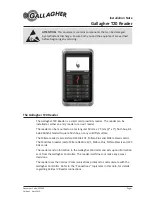
T20
Brand: Gallagher Pages: 13

PUC2
Brand: Yellowtec Pages: 11

PEX3U3F800
Brand: StarTech.com Pages: 10

WDT1000-P
Brand: ICS Advent Pages: 34

AC5426P
Brand: AXIOMTEK Pages: 36

Payter
Brand: E-Service Pages: 9

Imperial Digiplex Evo R915
Brand: Paradox Pages: 4

Video-PX7600GS-256
Brand: Jaton Pages: 25

PCI-IDO-16A
Brand: Acces I/O products Pages: 19

BR651
Brand: Videofied Pages: 6

Revolution 7.1
Brand: M-Audio Pages: 41

Dman PCI
Brand: M-Audio Pages: 52

V6600LE-512P
Brand: Diablotek Pages: 1

Javelin S884
Brand: Symmetry Pages: 2

NEO RF245
Brand: IDTECK Pages: 14

MR100
Brand: Sigur Pages: 52

All-in-1 USB 3.0
Brand: US Robotics Pages: 6

V680-CA1D
Brand: Omron Pages: 113


