DVD-VCR COMBINATION
SV-DVD3E
SV-DVD6E
SERVICE
1. Precautions
2. Product Specifications
3. Disassembly and Reassembly
4. Alignment and Adjustment
5. Troubleshooting
6. Exploded View and Parts List
7. Electrical Parts List
8. Block Diagram
9. PCB Diagrams
10. Schematic Diagrams
Manual
DVD-VCR COMBINATION
CONTENTS
SERVICE MANUAL
SV
-DVD3E/SV
-DVD6E
© Samsung Electronics Co., Ltd.
MAR. 2002
Printed in Korea
AK82-00198A
EJECT
SELECT COPY
REC
CHANNEL
VIDEO
L
AUDIO R
OPEN/CLOSE
STANDBY/ON
AUX
SELECT COPY
CHANNEL REC
EJECT
OPEN/CLOSE
L
AUDIO R
VIDEO
AUX
STANDBY/ON
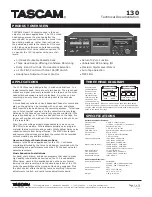
SV-DVD3E
SV-DVD6E
ELECTRONICS
For mechanical disassembly and adjustment, refer to the “Mechanical Manual” (TS-10A AC82-00023A).
Summary of Contents for SV-DVD3E
Page 7: ...Product Specifications 2 2 Samsung Electronics MEMO ...
Page 39: ...Troubleshooting 5 20 Samsung Electronics MEMO ...
Page 49: ...Exploded View and Parts List 6 10 Samsung Electronics MEMO ...
Page 60: ...Samsung Electronics 8 1 8 Block Diagram ...
Page 61: ...Block Diagram 8 2 Samsung Electronics MEMO ...
Page 63: ...PCB Diagrams 9 2 Samsung Electronics 9 1 VCR Main COMPONENT SIDE ...
Page 64: ...PCB Diagrams 9 3 Samsung Electronics CONDUCTOR SIDE ...
Page 65: ...PCB Diagrams 9 4 Samsung Electronics 9 2 DVD Main COMPONENT SIDE SOLDER SIDE ...
Page 66: ...PCB Diagrams 9 5 Samsung Electronics 9 3 Function Timer COMPONENT SIDE CONDUCTOR SIDE ...
Page 67: ...PCB Diagrams 9 6 Samsung Electronics MEMO ...
Page 70: ...Schematic Diagrams 10 3 Samsung Electronics 10 1 S M P S ...
Page 71: ...Schematic Diagrams 10 4 Samsung Electronics 10 2 Power Drive ...
Page 72: ...10 3 Function Timer Schematic Diagrams 10 5 Samsung Electronics ...
Page 73: ...Schematic Diagrams 10 6 Samsung Electronics 10 4 System Control Servo ...
Page 74: ...Schematic Diagrams 10 7 Samsung Electronics 10 5 A V ...
Page 75: ...Schematic Diagrams 10 8 Samsung Electronics 10 6 Hi Fi MTS ...
Page 76: ...Schematic Diagrams 10 9 Samsung Electronics 10 7 Input Output ...
Page 77: ...Schematic Diagrams 10 10 Samsung Electronics 10 8 A2 NICAM ...
Page 78: ...Schematic Diagrams 10 11 Samsung Electronics 10 9 OSD VPS PDC ...
Page 79: ...Schematic Diagrams 10 12 Samsung Electronics 10 10 SECAM ...
Page 80: ...Schematic Diagrams 10 13 Samsung Electronics 10 11 TM ...
Page 81: ...Schematic Diagrams 10 14 Samsung Electronics 10 12 DVD Main Micom AV Decoder ...
Page 82: ...Schematic Diagrams 10 15 Samsung Electronics 10 13 DVD Servo ...
Page 83: ...Schematic Diagrams 10 16 Samsung Electronics 10 14 DVD Audio Video ...