background image

ORDER NO.

PIONEER CORPORATION

   4-1, Meguro 1-chome, Meguro-ku, Tokyo 153-8654, Japan

PIONEER ELECTRONICS SERVICE, INC.  P.O. Box 1760, Long Beach, CA 90801-1760, U.S.A.
PIONEER ELECTRONIC NV  Haven 1087, Keetberglaan 1, 9120 Melsele, Belgium
PIONEER ELECTRONICS ASIACENTRE PTE. LTD.  253 Alexandra Road, #04-01, Singapore 159936


PIONEER CORPORATION 2000

c

X-MDX717

RRV2384

1. SAFETY INFORMATION ...................................... 2

2. EXPLODED VIEWS AND PARTS LIST ............... 3

3. BLOCK DIAGRAM AND SCHEMATIC DIAGRAM ... 18

4. PCB CONNECTION DIAGRAM ......................... 40

5. PCB PARTS LIST ............................................... 53

6. ADJUSTMENT .................................................... 60

CONTENTS

7. GENERAL INFORMATION ................................ 64

    7.1 DIAGNOSIS .................................................. 64

       7.1.1 TROUBLESHOOTING ........................... 64

       7.1.2 DISASSEMBLY/ASSEMBLY .................. 73

    7.2 PARTS .......................................................... 82

       7.2.1 IC ............................................................ 82

       7.2.2 DISPLAY ................................................. 86

8. PANEL FACILITIES AND SPECIFICATIONS ....... 89

T – ZZR  SEPT. 2000 Printed  in Japan
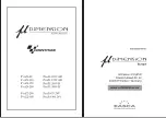
XR-MDX717

MD/CD COMPONENT SYSTEM

Type

Model

Power Requirement

Remarks

X-MDX717

LBXCN

AC110V

NLWXCN/HK

AC220V

THIS MANUAL IS APPLICABLE TO THE FOLLOWING MODEL(S) AND TYPE(S).

This product is a system(s) component.

Component

Model

Service manual

Remarks

X-MDX717

STEREO MD/CD CASSETTE DECK RECEIVER

XR-MDX717

RRV2384

This manual.

SPEAKER SYSTEM

S-C3-S-LR

RRV2391

0

PUSH OPEN

STEREO  MD/CD  DECK  RECEIVER  SYSTEM XR-MDX717

CD1

COLOR SELECTER

LINE IN

CD2

CD3

3-DISC  MULTI  CD  PLAYER

LINE

TAPE

MD

CD

TUNER

EASY  OPERATION SYSTEM  MD  SYSTEM

AUTO  REVERSE

STEREO  CASSETTE  TAPE  DECK

7

¡

1

Summary of Contents for X-MDX717

Page 1: ...IAGNOSIS 64 7 1 1 TROUBLESHOOTING 64 7 1 2 DISASSEMBLY ASSEMBLY 73 7 2 PARTS 82 7 2 1 IC 82 7 2 2 DISPLAY 86 8 PANEL FACILITIES AND SPECIFICATIONS 89 T ZZR SEPT 2000 Printed in Japan XR MDX717 MD CD COMPONENT SYSTEM Type Model Power Requirement Remarks X MDX717 LBXCN AC110V NLWXCN HK AC220V THIS MANUAL IS APPLICABLE TO THE FOLLOWING MODEL S AND TYPE S This product is a system s component Component...

Page 2: ...ay void the warranty If you are not qualified to perform the repair of this product properly and safely you should not risk trying to do so and refer the repair to a qualified service technician IMPORTANT THIS PIONEER APPARATUS CONTAINS LASER OF CLASS 1 SERVICING OPERATION OF THE APPARATUS SHOULD BE DONE BY A SPECIALLY INSTRUCTED PERSON LASER DIODE CHARACTERISTICS OF CD PLAYER MAXIMUM OUTPUT POWER...

Page 3: ... NSP are generally unavailable because they are not in our Master Spare Parts List The mark found on some component parts indicates the importance of the safety factor of the part Therefore when replacing be sure to use parts of identical designation Screws adjacent to mark on product are used for disassembly NOTES 2 1 PACKING Mark No Description Part No Mark No Description Part No 5 XR MDX717 1 1...

Page 4: ...L PWB 6 25 14 7P 14P 15P 10P 9 10 25 Insulation Plate 12 11 25 8 5 8 1 1 A A 1 17 1 24 2 24 7 19 18 24 2 20 3 23 22 26 21 Refer to 2 4 FRONT UNIT SECTION Refer to 2 3 UNIT ASSY 2 2 SECTION Refer to 2 6 MD UNIT SECTION Refer to 2 5 TOP PANEL ASSY SECTION F G ...

Page 5: ...1903 12 15P CON ASSY CN455 C488151904 13 14 7P CON ASSY C48F070811 15 16 17 CD Label 1028070050 18 ANT Caution Label 9A10000770 19 SP Caution Label 9A10000800 20 Spacer 2041070050 21 SP Light Label 9A10000820 22 4P CON ASSY C48F040811 23 SP SOCKET PWB ASSY C142279320 24 Screw BCZ30P060FZK 25 Screw BBZ30P060FMC 26 Lasser Caution Label 9A10000830 2 CONTRAST TABLE XR MDX717 LBXCN and NLWXCN HK are co...

Page 6: ... 32 35 33 34 31 29 3 3 41 1 23 21 21 21 21 47 18 19 45 20 16 44 46 17 17 22 15 2 25 X FORMER PWB 2 42 42 28 2 5 7 IC PWB 6 6 11 4 49 13 14 DI PWB AMP PWB 10 8 8 7 28 43 43 38 2 29 CD PWB Double Face 39 48 Double Face 6 49 52 9 51 50 12 Refer to 2 11 CD MECHA SECTION H B I 2 3 UNIT ASSY 2 2 ...

Page 7: ...51 34 Wire Connector 9P CN804 C488091910 35 Wire Connector 6P CN802 C48P063512 36 CD Mecha Cover 2012070050 37 FFC 16P CD CD Mecha 5421609024 38 Himelon B 2037070050 39 FFC 19P CD CONTROL 5421931004 40 FFC 23P CD CONTROL 5422332024 41 Bottom Chassis 1017070050 42 Screw BSZ26P050FMC 43 Cushion D 2039070050 44 Fuse F501 See Contrast table 2 45 Fuse F502 T5A 5267500L62 46 Fuse F503 T2 5A 5267250L62 4...

Page 8: ...X MDX717 XR MDX717 2 4 FRONT UNIT 1 10 4 5 12 7 8 38 35 21 13 3 17 16 37 22 35 32 36 36 34 23 27 6 33 30P 14P 2 10 20 19 11 14 25 36 37 37 37 36 36 36 41 18 27 X5 26 39 40 15 42 28 36 36 31 29 3P 37 K L J ...

Page 9: ... Knob CD 1 Assy 0002070050 17 Disc Knob CD 2 Assy 0003070050 18 Disc Knob CD 3 Assy 0004070050 NSP 19 Front Panel 1001070050 20 Volume Knob 1009070050 21 Power Knob 1010070050 22 MD Eject Knob 1011070050 23 Cushion C 2042070050 24 NSP 25 JACK PWB ASSY C143279130 26 Color Jog 1012070050 27 Edit Knob 1013070050 28 Knob Holder A 2013070050 29 3P CON Assy C48P031811 30 31 Cushion A 2026070050 32 FRONT...

Page 10: ... CONT 5421924024 3 TUNER PWB ASSY C142279800 4 Connector Plate 2029070050 5 5P CON ASSY C48P051011 6 6P CON ASSY C48P061011 7 DECK PWB ASSY C141279600 8 9P CON ASSY C48P090811 9 Earth Terminal 2044070050 10 Screw BPZ30P100FMC 11 Gear Damper 2000001269 12 13 Deck Mecha CRL3423 14 Lock Lever 2006070050 15 16 COM Spring 2016070050 17 Door Spring 2015070050 18 Top Panel 1002070050 19 Deck Door Assy 00...

Page 11: ...R213 R142 is removed from KMK 260AAB Mark No Description Part No 1 Screw BSZ26P050FMC 2 MD Mecha KMK 260AAB GXX1155 3 MD Mecha Chassis 2018070050 4 MD Shield Case 2019070050 5 MD Door 1021070050 6 Shaft 2020070050 7 EXT Spring 2021070050 8 9 11P CON ASSY C48P111811 10 FFC 11P MD CONT 5421116024 11 FFC 19P MD MD Mecha 5421906024 12 FFC 16P MD MD Mecha 5421606024 13 Shield Plate 2022070050 14 MD PWB...

Page 12: ... Plate D 500934311 11 Cap Reel 502284020 12 Gear Reel 502224006 13 Lever ST 502594041 14 Guide C 502194014 15 Lever Brake 502593040 16 Frame A 502113013 17 ARM SW 502394027 18 ARM CS 502394026 19 Assy Chassis 500934099 20 Screw GSE10A2003 21 Spring 010824650 22 Spring 010804649 23 Spring 010814601 24 Screw GSE20A2005 25 Spring 010804635 26 Spring 010824599 27 Spring 010804607 28 Spring 010824651 2...

Page 13: ...ch 500934069 11 ARM UD A 502394017 12 Gear UD 502224007 13 Pulley D 502234254 14 Belt FR 020834188 15 Assy Flywheel RA 500933312 16 Belt SR 020844200 17 Bracket MM 501193073 18 Assy Motor 500934328 19 Wire M M 160724055 20 Assy PWB 500934345 21 PWB 500703107 22 9P Housing S9BPH K S 23 Spring Switch 010824646 24 Photo Interrupter SG211V 25 Resistor ERDS2TJ471 26 Mode Switch MSW17220MVQO 27 Spacer 5...

Page 14: ...646 248 2 11 Insulator 2 646 548 01 12 Screw 7 688 002 11 13 Screw Step 4 628 167 01 NSP 14 Frame Slide 2 646 557 01 15 Arm Head 2 646 559 01 16 Spring Tension Coil 2 646 562 01 Slot Frame 17 Spring SP Tension 2 646 561 01 Arm Head 18 Cam Mode 2 646 560 01 19 PWB Head Flexible 1 669 181 11 20 Grip P1 7 2 5TYPE2 2 627 529 01 21 Over Write Head 1 550 518 12 NSP 22 Sheet Double Fase 2 646 549 02 NSP ...

Page 15: ...ble 1 669 180 11 NSP 9 Wire SL Motor Lead 1 783 318 11 NSP 10 Wire SL Motor Lead 1 783 318 21 11 Shaft Guide 2 646 452 01 12 Grip P1 4 1 4TYPE2 2 627 530 01 13 Rack Inserter 4 963 914 02 14 Plate Pre Road 2 646 567 01 15 Screw 1 2 3 3 2 627 431 01 16 SL Motor Assy X 2626 329 1 17 Gear MD 2 646 571 01 18 Screw P1 7 4 TYPE3 7 627 852 18 19 SP Motor Assy X 2626 327 1 20 Lead Screw Assy X 2626 330 1 2...

Page 16: ...14 15 68 72 17 16 66 71 43 79 46 44 43 46 43 31 27 8 9 9 4 6 50 51 80 48 24 21 40 39 39 71 25 67 66 26 22 33 49 38 53 23 52 3 7 53 71 52 2 7 29 58 61 37 69 18 66 77 61 58 64 34 59 62 56 60 52 5 7 11 13 10 63 35 1 60 52 4 7 53 20 36 59 55 54 52 7 7 52 6 7 54 52 1 7 73 3 2 11 CD MECHA ...

Page 17: ... 45 229 3069 33 Pulley A 45 222 4052 NSP 34 Pulley Motor 23 226 4031 NSP 35 Pulley Motor 23 226 4096 36 Spring 01 000 4541 37 Spring 01 082 4558 38 Spring 01 082 4559 39 Belt 02 083 4157 40 Belt 02 083 4152 41 Cushion 45 063 4136 42 Frame S 45 211 3072 43 Rubber Cushion SO 45 063 4072 44 Pick up Unit KSM213CCM 45 Spring 01 081 4561 46 Spring 01 081 4562 47 Assy Carriage 200 45 093 4190 48 Assy Car...

Page 18: ...NA REG IC305 BA15218N ALC IC302 BA335 Q311 2SC2001 TPSS BIAS IC2 415309216P TC9216P PLL IC1 415302099N TA2099N FM IF DET MPX AM RF IF DET FE1 TFFJ2U573A FM TUNER MODULE L1 ANT COIL 4300103280 Q2 2SK193 AM RF TUNING Q1 2SC1675L RF AMP IC504 NJM4558 BUFFER CF 3 AM OSC CF 1 IC802 CXD2589Q 415C02589Q D S P PROCESSOR IC801 415C01992R CXA1992BR RF AMP FOCUS TRACKING SERVO IC803 4159059360 BA5936S POWER ...

Page 19: ...GHT LED REMOCON REC RM700 7140500001 SPS 444 1 MUTE Q152 Q252 2SC2001 S MUTE TUNER 9V Q150 Q250 2SC2001 H P AMP IC400 BA15218N POWER AMP IC401 4152046630 LA4663 POWER AMP CONT ST BY AND MUTE Q417 2SC945P Q418 DTA114TS Q401 2SA966 CD 7 8V AUDIO REG 8V MD 5V IC402 415920RX11 PQ20RX11 TUNER 5V Q400 2SC2001 Q403 Q404 Q407 2SC945P Q406 4100013890 2SA1389 D423 4130G5SBA2 KBU603 D424 D427 4120154020 1N54...

Page 20: ...VSYS 5VSYS 512FS HGND 256FS BCK MGND DADT M 5V LRCK M 5V GSYS 1 2 3 4 5 6 7 8 9 10 11 12 13 14 15 16 1 2 3 4 5 6 7 8 9 10 11 12 13 14 15 16 LEDO RXD TXD RTS CTS SCLK SWDT EMPHASIS STB VBAT P DOWN AMUTE XLATCH SYS RST SYS 3 3V DARST 1 2 3 4 5 6 1 2 3 4 5 6 SP CARR DRAW DRAW CARR 1 2 3 4 5 6 7 8 9 1 2 3 4 5 6 7 8 9 REC R REC F HALF CrO 2 PHOTO Rch COM GND E HEAD GND SOLENOIDO VCC MODE P GND 1 2 3 4 ...

Page 21: ...00 NLWXCN HK TYPE C142279501 1 2 3 4 5 6 7 8 9 10 11 12 13 14 1 2 3 4 5 6 7 8 9 10 11 12 13 14 15 16 17 18 19 20 21 22 23 24 25 26 30 29 28 27 26 25 24 23 22 21 20 19 18 17 16 15 14 13 12 11 10 9 8 7 6 5 REMOCON DISC3 DISC2 DISC1 VJOG0 CJOG0 VJOG1 CJOG1 VCC GND KEY1 KEY0 KEY2 KEY3 LEDVCC LEDGND LCDGND RS RW E NC NC DB0 DB1 LCDGND LCDVCC VSOUT RS RW E DB0 DB1 DB3 DB2 DB4 DB5 DB6 DB7 1 2 3 4 5 6 7 8...

Page 22: ...0 10 C56 4 7 50 C38 22 16 C37 0 01 C42 100 10 1 3 6 4 L2 MW OSC COIL C46 100p C43 1000p C47 100p C48 100p C44 33p C45 33p 8 7 6 5 4 3 2 1 9 10 11 12 13 14 15 16 T CH CH CH CH CH 1 2 3 4 R2 82 R4 100k R3 330 4160200003 41065193TP 4120103480 4330102020 4153092169 4300103280 4160200003 41091114YS CF1 10 7MA C74 0 01 C72 0 022 T L8 22µH CF3 10 7MA R6 10 C2 0 022 L7 22µH R5 330 C5 1000p T C54 0 01 T C7...

Page 23: ...0 068 C25 0 1 50 C26 1 50 R24 2 2k R65 22k R25 3 9K C28 0 015 M C51 0 01 T R27 2 2k C29 1000p T C31 4 7 50 C32 4 7 50 R28 2 2k C30 1000p T C19 0 015 M R26 3 9k R20 10k R58 10k C15 0 01 T C13 4 7 50 R69 2 7k C12 0 01 T R19 55 R18 4 7k R17 47k C55 1 50 R66 3 3k R52 10k R51 1k R50 2 2k R49 2 2k R48 1k R53 10k C80 270p PERIOD CLOCK DATA TUNING ST L CH GND R CH 5V 9V RDS OMLY RF IN FM BW VL SENS AM OSC...

Page 24: ...M CARM DRWE DRWE TEO LPFI TEI ATSC TZC TOFCT VC FZC SL_P SL_M SL_O ISET VCC LOCK CLK XLT DATA XRST C OUT SENS1 SENS2 FE_BIAS M SPINDLE CARRIAGE M SLED LOADING LIMIT SW S05 3 3 1 2 3 4 1 2 3 4 1 2 3 4 5 6 7 8 9 10 11 12 13 14 15 16 32 31 30 29 28 27 26 25 24 23 22 21 20 19 18 17 M M 1 1 2 2 4 4 IC803 BA5936S 4159059360 IC804 NJM4558M OUT1 OUT2 OUT1 OUT2 IN2 IN1 VCC VCC REG I REG B REG OUT IN3 R IN3...

Page 25: ...6 CLK P76 XCK P75 DATA P80 XRST P82 SENS P77 SQCK P81 MUTE P69 SQSO P79 NC HP SW HP L CH HP GND HP R CH LINE B LINE IN L CH LINE IN GND LINE IN R CH D GND LINE IN_RCH LINE IN_GND LINE IN_LCH B HP_RCH HP_GND HP_LCH HP_SW CD_RCH CD_GND CD_LCH PW GND PW GND 7 5V 7 5V CD_FUNC SW D OUT D GND NC LOCK P28 M_GND SW2 SW3 SW4 SW5 SW6 SW7 SW8 R840 160k R841 160k R842 160k R843 270k R844 270k R845 270k R845 2...

Page 26: ...X MDX717 XR MDX717 26 A B C D 1 2 3 4 1 2 3 4 3 5 MD PWB ASSY C MD PWB ASSY C143279001 C CN103 D CN102 CN501 CN502 D MD MD MDREC MDREC MDREC MDDI MDDI MDDI MDREC MD MD MDREC MD ...

Page 27: ... F 2 2 MD AUDIO SIGNAL ROUTE EF501 EF512 EMIFIL DSS306 55B101M100 7080055001 MD MD REC ANALOG AUDIO SIGNAL ROUTE MDREC MD REC FROM CD DATA AUDIO SIGNAL ROUTE MDDI MD MD MDREC MDREC MDDI MDDI MDDI MD FB548 FB551 FB553 FB558 CHIP BEAD MF1310211D FB561 FB565 FERRITE BEAD 7089710001 ...

Page 28: ...FO MORFI RFO OPN OPO ADDC COMPP COMPO AGC1 RFAGC RF PEAK ILCC MOD VR PD K FCS FCS TRK TRK CAPA CAPA IN2R IN2F VM2 OUT2F PGND2 OUT2R VM12 OUT1R PGND1 OUT1F VM1 IN1F IN1R VDD GND VG IN4R IN4F VM4 OUT4F PGND4 OUT4R VM34 OUT3R PGND3 OUT3F VM3 IN3F IN3R PSB 21 20 19 18 17 16 15 14 13 12 11 10 9 8 7 6 5 4 3 2 1 I 3V IOP TE VC RF 5 4 3 2 1 SLED SLED SPDL SPDL PROTECT GND REFLECT 7 6 5 4 3 2 1 C115 0 22 1...

Page 29: ...OSC1 OSC0 XISL RVDD RVSS DIN DOUT ADDT DADT LRCK MVC1 D3 D2 D0 D1 XWE XRAS A09 XCAS XOE DVSS A11 A08 A07 3 3V GND REFLECT PROTECT LIMITIN LDIN LDOUT AMUTE XLATCH SCTX XSCTX MOD DA RST DIG RST A06 A05 A04 A10 A00 A01 A02 A03 DVDD 256FS XBCK AUX2 TE SE AVSS ADRB ADRT AVDD ADIO VC AUX1 FE ABCD BOTM PEAK CLTV FILO FILI PCO PDO AVSS RF1 BIAS AVDD ASYI GND XIN 1 XOUT 1 VBAT 3 3V TEST SYSTEM RST DQSY SQS...

Page 30: ...SC945P Q308 2SC945P Q324 2SC945P Q311 2SC2001 Q305 DTC114TS Q302 2SC2001 Q303 2SC2001 R101 560k R201 560k R102 47k R202 47k R103 47k R203 47k C103 100p C203 100p C102 1000p C202 1000p T T T T 2 3 1 6 5 4 1 2 3 4 5 6 7 8 9 10 11 12 13 14 15 16 17 18 19 C101 1 50 C201 1 50 C301 4 7 50 L301 4330802220 M T M M T T T T T T M M M C302 0 027 C344 0 1 C304 47 16 C308 1 50 C312 10 50 C311 1 50 C316 1 50 C2...

Page 31: ... D201 1SS133 D101 1SS133 R128 470k R137 6 8k R328 10k R338 220 R139 10k R239 10k Q108 2SC945P Q208 2SC945P Q206 2SC945P Q106 2SC945P Q207 2SC2001 Q107 2SC2001 Q204 DTC114TS Q104 DTC114TS 1 2 1 2 1 2 1 2 C227 0 018 C127 0 018 C317 47 16 C225 2 2 50 C125 2 2 50 C226 4 7 50 C126 4 7 50 C333 1 50 C335 470 10 C336 1 50 C330 22 16 C328 1000p C329 1000p C326 47 16 C343 1 50 C332 100 16 C314 100 16 Q318 D...

Page 32: ...650A 1 50 C750A 1 50 GND R_CH GND L_CH 8V HP_RCH HP_GND HP_LCH HP_SW CD_RCH CD_PREGND CD_LCH CD_GND CD_GND CD 7V CD 7V FCD MD_DIN CD_GND CN450 DECK_SW0_1 DECK_SW2_3 MOTOR BEAT_CUT REC_PLAY SOLENOIDE REPEAT PHOTO TPSS BIAS REC_MUTE AUDIO_GND R_PB_OUT AUDIO 8V L_PB_OUT 11V R_REC_IN PRE_GND L_REC_IN CN453 TUNER 9V TUNER 5V TUNER_RCH TUNER_GND TUNER_LCH CN451 RCH_OUT MD A GND LCH_OUT MD M GND MD M GND...

Page 33: ...CN472_ 18 NC 19 L2 20 NC 21 L1 22 VSS 23 CL 24 DI 25 CE 26 VSS 27 AVSS 28 R1 29 NC 30 R2 31 NC 32 R3 64 LF5 63 LVREF 62 LINVIN2 61 LTOUT 60 LVRIN 59 NC 58 LVROUT 57 VDD 56 VREF 55 RVROUT 54 NC 53 RVRIN 52 RTOUT 51 RINVIN2 50 RVREF 49 RF5 16 R4 15 RINVIN1 14 RSELO 13 RTIN 12 RF1C1 11 RF1C2 10 RF1C3 9 RF2C1 8 RF2C2 C763 0 22 C764 0 068 C767 0 0027 C768 680p C765 0 022 C766 0 0047 C769 0 0015 C770 39...

Page 34: ...73 100k D907 D901 5 1V 31 SOUND_CE IC900 CXP740096 122Q FB917 JW2 JW3 JW4 JW5 L905 10U L903 10U FB910 10U CN459 PERIOD CLOCK T DATA TUNING STEREO NC CN458 Q936 2SD1757K SA301757KS Q929 2SD1757K SA301757KS D907 LL4148 SD14148G08 Q936 A_ Q929 Q921 2SD1757K SA301757KS Q905 2SD1757K SA301757KS Q915 2SD1757K SA301757KS Q917 2SC2412K Q925 2SD1757K SA301757KS Q927 2SC2412K 32 SOUND_DI 33 SOUND_CL 34 S_MU...

Page 35: ...A 79 80 1 2 3 4 1 2 3 4 DI CE DECKMUTE FAUX VSS DIN ELCONT 11V SMUTE BEEP FCD FTUNER PSCONT ACDET EL EL REPEAT PHOTO MOTOR SOLENOID DECKSW0 1 DECKSW2 3 BEATCUT TPSS RECMUTE RECPLAY BIAS VSS CL CN700 1 2 K F C518 1000 6 3 C511 10 35 C964 0 22 5 5 C985 47 16 C978 220 6 3 C977 220 6 3 C502 1 C519 1 C999 1 1 3 1 3 2 2 C984 1 C981 0 1 C982 1000p C983 1 C979 1 C980 1 C500 1 C961 1 R528 1k R527 1k R505E ...

Page 36: ...MDX717 36 A B C D 1 2 3 4 1 2 3 4 H 3 10 AMP and X FORMER PWB ASSYS I X FORMER PWB ASSY I AMP PWB ASSY LBXCN C1422797711 NLWXCN HK C142279710 H CN455 CN406 CN400 WC601 F 1 2 A LBXCN C142279500 NLWXCN HK C142279501 ...

Page 37: ...X MDX717 XR MDX717 37 A B C D 5 6 7 8 5 6 7 8 H CN454 CN405 CN401 CN403 SPEAKER F 1 2 AUDIO SIGNAL ROUTE HP AUDIO SIGNAL ROUTE HP HP HP HP HP A F 1 2 K H ...

Page 38: ...X717 38 A B C D 1 2 3 4 1 2 3 4 FRONT A PWB ASSY C143279110 K JACK PWB ASSY C143279130 J CN461 F 2 2 CN465 LCD PANEL LC700 F 2 2 CN807 B HP LINE IN LINE IN HP HP LINE IN HP 3 11 JACK FRONT A and FRONT B PWB ASSYS J K ...

Page 39: ...ASSY C143279120 L FRONT B PWB ASSY S700 STAND BY ON S701 0 CD 1 S702 0 CD 2 S703 0 CD 3 S704 CD 1 S705 CD 2 S706 CD 3 S715 0 MD EJECT FRONT A PWB ASSY S707 S708 TUNER S709 CD S710 MD S711 TAPE S712 LINE S713 7 STOP S714 1 S716 COLOR S717 EDIT S718 TIMER S721 REC MODE S722 DEL DISP S723 ENTER Jog controler EN701 COLOR SELECTOR EN700 VOL DOWN UP L K ...

Page 40: ...parts of PCB and schematic diagrams is shown below 3 The parts mounted on this PCB include all necessary parts for several destinations For further information for respective destinations be sure to check with the schematic diagram 4 View point of PCB diagrams Symbol In PCB Diagrams Symbol In Schematic Diagrams Part Name Transistor Transistor with resistor Field effect transistor Capacitor Connect...

Page 41: ...X MDX717 XR MDX717 41 A B C D 1 2 3 4 1 2 3 4 4 2 MD PWB ASSY C MD PWB ASSY C MD PWB ASSY C SIDE A SIDE B CN103 D CN102 D CN460 F CN452 F IC505 Q504 Q502 Q503 IC504 IC501 IC503 IC502 Q501 ...

Page 42: ...X MDX717 XR MDX717 42 A B C D 1 2 3 4 1 2 3 4 B 4 3 CD PWB ASSY CD PWB ASSY B SIDE A CN450 F CN807 J CN459 F CD MECHA CD MECHA CD MECHA IC803 IC804 IC801 Q801 IC802 Q802 Q804 ...

Page 43: ...X MDX717 XR MDX717 43 A B C D 1 2 3 4 1 2 3 4 B CD PWB ASSY B SIDE B ...

Page 44: ...X MDX717 XR MDX717 44 A B C D 1 2 3 4 1 2 3 4 D 4 4 MD MOUNT IC122 IC201 Q105 Q103 D102 MD MECHANISM CN502 C CN501 C IC122 IC201 Q105 Q103 MD MECHANISM MD MOUNT D SIDE A ...

Page 45: ...3 Q162 Q104 Q102 IC171 IC125 IC103 IC202 IC181 IC152 IC123 IC121 Q163 Q104 IC123 IC101 IC125 IC171 IC103 IC202 R142 R123 R213 IC181 Q101 Q162 Q102 IC152 Q181 Q182 IC121 NOTE GXX1155 is MD mechanism for service by which resistance R123 R213 R142 is removed from KMK 260AAB MD MOUNT D SIDE B ...

Page 46: ...C D 1 2 3 4 1 2 3 4 F 4 5 CONTROL and SP SOCKET PWB ASSYS G CONTROL PWB ASSY F SP SOCKET PWB ASSY G SIDE A CN700 K CN701 K CN458 A CN302 E CN401 CN405 H CN400 CN406 H CN805 B CN806 B CN503 C CN504 C CN451 A IC452 Q456 Q928 Q651 ...

Page 47: ... A B C D 1 2 3 4 1 2 3 4 G F CONTROL PWB ASSY F SP SOCKET PWB ASSY G SIDE B Q904 Q903 Q914 Q911 Q913 Q937 Q935 Q933 Q931 Q917 IC900 Q912 Q915 Q901 IC901 Q902 Q923 Q921 Q925 Q927 Q450 IC450 Q457 Q750 Q850 Q920 Q936 Q451 Q450 ...

Page 48: ... 2 3 4 4 6 DECK PWB ASSY E DECK PWB ASSY D SIDE A CN453 F DECK MECHA DECK MECHA Q201 Q311 Q308 Q317 Q106 Q107 Q321 Q323 Q325 Q322 Q310 Q320 Q202 Q313 Q324 Q318 Q104 Q204 Q206 Q207 IC301 IC302 Q301 Q305 Q312 Q108 Q208 Q103 Q102 Q101 Q203 Q314 ...

Page 49: ...717 XR MDX717 49 A B C D 1 2 3 4 1 2 3 4 H 4 7 AMP PWB ASSY AMP PWB ASSY H SIDE A CN454 F SPEAKER WC601 I CN455 F IC402 IC401 Q406 Q252 Q152 Q417 Q418 Q403 Q404 Q150 Q250 Q415 Q400 Q402 IC403 Q401 IC400 Q407 ...

Page 50: ...X MDX717 XR MDX717 50 A B C D 1 2 3 4 1 2 3 4 4 8 JACK FRONT A and FRONT B PWB ASSYS J K L CN807 B FRONT A PWB ASSY K FRONT B PWB ASSY L JACK PWB ASSY J SIDE A CN465 F LCD PANEL LC700 Q809 IC504 Q810 ...

Page 51: ...X MDX717 XR MDX717 51 A B C D 1 2 3 4 1 2 3 4 L K J FRONT A PWB ASSY K FRONT B PWB ASSY L JACK PWB ASSY J SIDE B CN461 F Q701 Q708 Q703 Q705 Q700 Q702 ...

Page 52: ...X MDX717 XR MDX717 52 A B C D 1 2 3 4 1 2 3 4 I 4 9 X FORMER PWB ASSY CN403 H AC IN NEUTRAL LIVE X FORMER PWB ASSY I SIDE A ...

Page 53: ...factor of the part Therefore when replacing be sure to use parts of identical designation When ordering resistors first convert resistance values into code form as shown in the following examples Ex 1 When there are 2 effective digits any digit apart from 0 such as 560 ohm and 47k ohm tolerance is shown by J 5 and K 10 Ex 2 When there are 3 effective digits such as in high precision metal film res...

Page 54: ...QYB223K50 C874 C875 C877 C880A C880B C891 CKSQYB223K50 C802 C804 C826 CKSQYB333K50 C811 CKSQYB472K50 C814 CKSQYB473K50 C851 CKSQYB562K50 C813 CKSQYB682K50 C829 CKSQYB683K25 RESISTORS R801 R834 RD1 4PU100J R850 RD1 4PU102J R853 R878 R879 RD1 4PU103J R813 R818 RD1 4PU104J R852 RD1 4PU153J R854 RD1 4PU223J R880 RD1 4PU331J R851 R858 R876 RD1 4PU473J R873 RD1 4PU511J Other Resistors RS1 10S J OTHERS C...

Page 55: ...01 CEAT1R0M50 C204 C208 C210 C220 C308 C311 CEAT1R0M50 C315 C316 C333 C336 CEAT1R0M50 C112 C330 CEAT220M50 C125 C225 CEAT2R2M50 C304 C305 C317 C326 C342 CEAT470M16 C319 C335 CEAT471M10 C126 C226 C301 CEAT4R7M50 C313 CEATR47M50 C343 CEAL1R0M50 C318 CEAL2R2M50 C212 CEAL220M16 C102 C113 C202 C213 C328 C329 CKPUYB102K50 C344 CKPUYB104Z50 C116 C127 C216 C227 CQMA183J50 C106 C206 CQMA223J50 C302 CQMA273...

Page 56: ...681 R781 RD1 4PM132J R650 R750 RD1 4PM133J R654 R754 RD1 4PM153J R546 RD1 4PM332J R508 R510 R533 R583 R930 RD1 4PU102J R931 R935 R974 RD1 4PU102J R657 R757 RD1 4PU103J R713 R973 RD1 4PU104J R655 R755 RD1 4PU222J R917 405041045E R553 405041025E R900 RFA1 4PS100J R503F RD1 4PU103J Other Resistors RS1 10S J OTHERS CN450 CN453 FFC 19P TOP BASE 4491900363 CN451 PH 5P TOP BASE 4490501004 CN452 PH 11P TO...

Page 57: ...C BUSHING 2000000767 IC INSULATOR A 2048070050 IC INSULATOR B 2049070050 AWG 20 1007 BLK 120mm 4 53B4001211 AWG 24 1007 BLK 160mm 4 5346001618 AWG 24 1007 BLK 100mm 4 5346011011 X FORMER PWB ASSY FILTER Mark No Description Part No Mark No Description Part No LF601 AC LINE FILTER 70699200C1 CAPACITORS C515 SPARK KILLER 4700pF 400V 5106472P41 OTHERS A PIN TERMINAL 2000000843 601 WIRE HOLDER 44905002...

Page 58: ...426 95 Q101 Q163 DTA144EK Q103 Q104 DTC114EK Q102 2SA1037K Q182 2SK1764KYR 8 729 017 65 Q181 2SJ278MYTR 8 729 018 75 Q162 2SB798 T1DK AZQ7132 D181 D183 F1J6TP 8 719 046 87 D101 CHIP DIODE ARRAY DAN202K COILS L101 FERRITE BEED INDUCTOR 1 414 233 21 L FERRITE BEED INDUCTOR 1 414 235 11 L CHIP CONDUCTOR 2012 AZC7283 CAPACITORS C142 CCSQCH101J50 C106 CCSQCH102J50 C205 CCSQCH150J50 C105 CKSQYB103K50 C1...

Page 59: ...1 XTAL RESONETOR 12MHz 1 760 872 11 L SW MOUNT BOARD OTHERS FFC FPC CONNECTOR 6P 1 766 336 21 PUSH SWITCH 1KEY 1 771 092 21 PUSH REVER SW 1KEY 1 771 326 11 D SW MOUNT BOARD OTHERS 2PIN PUSH SW 2KEY 1 771 327 11 FFC FPC CONNECTOR 7P 1 779 345 11 Mark No Description Part No ...

Page 60: ... the adjustment ends B A PB L ch Oscilloscope X Y Mode Adjustment Screw FORWARD Side REVERS Side Top View Fig 1 Adjustment Points DECK UNIT CN453 PB R ch NCT 111 Playback 3 kHz adjustment screw No Mode Test Tape Adjusting Points Measurement Points Adjustment Value Remarks PLAY 1 JK805 Head Phone Jack 3000 Hz 90Hz 60Hz Plastic Driver Adjustment Screw Motor Fig 2 6 1 CASSETTE DECK SECTION Adjustment...

Page 61: ...annels unless otherwise specified 7 Warm up the unit for several minutes before adjustment In particular be sure to warm up the unit in the REC PLAY mode for 3 to 5 minutes before starting recording playback frequency characteristics adjustment 8 Always follow the indicated adjustment order Otherwise a complete adjustment may not be achieved Playback Adjustment 1 Head Azimuth Adjustment When the t...

Page 62: ...omes at maximum level 6 2 1 AM TUNER AECTION AM Tuner Section Set the mode selector to AM BAND Connect the wiring as shown in Fig 1 Note 1 For the area using 10kHz step frequency should be 1000kHz AM SG MPX SG FM SG PRODUCT DC Voltmeter FM75Ω antenna terminal AM antenna terminal 60cm Center Center Loop antenna Fig 1 AM and FM Adjustment Wiring Diagram Fig 2 Adjustment Point 6 2 TUNER SECTION T01 A...

Page 63: ...the adjustment of MD is not published 6 4 CD SECTION NOTE There is no information to be shown in this CD adjustment The adjustment of the part CD is a self adjustment The adjustment when picking up is exchanged is unnecessary Please reproduce usual CD and do the reproduction confirmation after exchanging picking up ...

Page 64: ...analog being sent to the output jack Please push 4 KEY or KEY Can you smoothly select music Is the audio signal digital being sent to the output jack OK Please record from CD to MD Please push CD PLAY PAUSE KEY or CD SELECT KEY of DISC No CD troubleshooting Please make the products to the power switching on and the CD mode Is CD DISC NO DISC displayed after CD DISC TOC READING is displayed on the ...

Page 65: ...e circuit of Q802 in the surrounding Crystal XTL801 is broken IC802 is broken Please check the circuit of XTL801 and IC802 in the surrounding 1 CD DISC NO DISC is displayed after CD DISC TOC READING is displayed on the LCD display and when the same operation do not repeat three times 2 How many seconds will it take by the time NO DISC is displayed from the chuckingclamp of DISC that SELECT is done...

Page 66: ...of IC801 Is the wave forms of Figure 4 shown with 1 pin FEO of IC801 Is the wave forms of Figure 5 shown with 2 pins FEI of IC801 Please check IC801 surrounding circuit and IC801 2 A Please check FFC wire connector CN801 from pick up IC802 IC803 Confirmation with solder of IC801 IC803 is broken Pick up is broken 27 of IC801 28 Confirmation with solder of 29 pins IC801 is broken IC801 is broken Ple...

Page 67: ... Is the wave forms of Figure 7 shown with 6 pins FEO of IC801 Please check the circuit of IC801 of 36 pins in the surrounding Please check a digital signal of 20 21 and 22 pins of IC801 Please check the FFC connector from pick up Pick up is broken Please check the circuit in the surrounding with the solder of IC801 of 17 pins IC801 is broken IC802 is broken Please check the circuit of IC801 IC803 ...

Page 68: ...f Figure 8 shown with 35 pins RF of IC802 Please check 29 30 and 31 pins of IC802 IC802 is broken Is 16 93MHz shown in 71 pins X TAL of IC802 Please check the circuit of 35 pins RF of IC802 and C857 in the surrounding IC802 is broken Please check the circuit in the surrounding with the solder of IC802 IC802 is broken 2 B wave form wave form ...

Page 69: ...7 pins TEI of IC801 Is the wave forms of figure 11 shown in 13 pins TAO of IC801 Is the wave forms of Figure 12 shown in 15 pins and 16 pins of IC803 Please check FFC connector CN801 IC801 is broken Please check the circuit of the TE line in the surrounding IC801 is broken Please check FFC connector CN801 Pick up is broken Please check the circuit of IC803 in the surrounding 2 C ...

Page 70: ...w 88 2KHz Do 41 pins PCMDI of IC802 show a digital signal Please check the circuit in the surrounding with the solder of IC802 and IC900 IC802 or IC900 is broken Please check the control unit and the amplifier unit Please check the circuit of IC802 in the surrounding IC802 is broken Please check the circuit in the surrounding with the solder of IC802 IC802 is broken 3 When the audio signal analog ...

Page 71: ...ase check the circumference circuit with the solder of 44 45 46 47 48 and 49 pins of IC801 4 When you cannot smoothly select music Please push 4 KEY or KEY Is the wave forms of Figure 13 shown with 1 pin of IC801 Please push 4 KEY or KEY Is the wave forms of Figure 14 shown with 13 pins of IC801 Please push 4 KEY or KEY Is the wave forms of Figure 15 shown with 19 pins of IC801 IC804 is broken ...

Page 72: ...l signal of H and L come from 53 pins DOUT of IC802 Please check the control unit and the MD unit Please check the circuit in the surrounding with the solder of IC802 IC802 is broken 5 When the audio signal digital is not sent to the output jack ...

Page 73: ...P PANEL ASSY Front Panel Assy Refer to page 74 FRONT PANEL Side Panel R 2 2 6 2 2 CONTROL PWB Assy 3 3 4 4 5 6 8 9 8 STANDBY ON Minus Driver Hook Tray Panel Take off 0 CD1 10 1 10 2 11 10 OR 7 1 2 DISASSEMBLY ASSSEMBLY CAUTION Please note static electricity at the FRONT PWB ASSY LC700 repair 1 The main body Side Panel R Remove as well as Side Panel L ...

Page 74: ...Unit Refer to page 75 MD MECHA Hook Right and Left x2 11 12 13 14 13 Bottom Side Refer to page 76 CD MECHA 1 2 2 2 1 2 2 2 CD MECHA Deck Bracket Deck Mecha TUNER PWB Assy 16 16 17 18 DECK PWB Assy 2 3 5 3 3 3 2 The CD mechanism is drawn out while pushing the hook 15 15 15 2 1 7 FRONT PANEL ASSY 7 TOP PANEL ASSY ...

Page 75: ... X MDX717 XR MDX717 4 7 MD MECHA 2 1 4 3 2 1 1 2 MD Shield Case Shield Plate MD Mecha Chassis 2 5 2 5 8 Flame Main 6 10 10 11 7 EXT Spring Tension Spring Door Arm MD Door Set MD MOUNT MD MOUNT MD Door Set ...

Page 76: ...inus driver and Drawer is drawn out Afterwards please remove Front Unit after removing Tray Panel Set 2 1 2 1 2 3 3 3 3 4 7 PICK UP UNIT CD MECHA CD Mecha Chassis Frame S The back of CD mecha Carriage 100 Method of distinguishing the back of Carriage Method of distinguishing surface of Carriage Carriage 200 Carriage 300 Carriage 100 1 Carriage 200 2 Carriage 300 3 7 CAUTION FOR DISASSEMBLY ASSSEMB...

Page 77: ...arriage 300 Chassis Drawer 7 DRAWER Thin minus driver etc Stops in the place of which it went out by about 1cm 4 to 7 The hook is removed The back of Chassis Drawer 1 2 3 4 5 6 7 9 8 CONNECTOR PCB 4 Carriage 300 is put in the Chassis side and please put in the Drawer side without fail in order of Carriage 100 and 200 ...

Page 78: ...el Gear4 Upper Pinion Black Cam Lower Pinion Mark of Pinion of both upper and lower must be a direction of black Cam Carriage 100 is No 1 carriage Carriage 200 is No 2 carriage After Bevel Gear is turned counterclockwise and five rotations are made after lower side Pinion begins to turn stops in the place where its rotation stopped 4 Carriage 200 3 The bottom of Carriage is hit under right Stopper...

Page 79: ...iage 100 drops below Carriage 200 is lightly lifted by the finger Note Lift it horizontally when you lift Carriage Carriage inclines when it is not the horizontal and mechanism locks Bevel Gear is turned clockwise direction of a rear side from a front side like the state of 9 Carriage 200 lifts up And when the movement is started Carriage 100 to the direction of a front side separates the hand whi...

Page 80: ...he lock comes off Slider 2 Direction of front Arm Stopper B Note Do not lift Arm Stopper B for above when you move Arm Stopper B There is a possibility to bend the spring when Arm Stopper B is lifted and the spring bends And when Arm Stopper B becomes floatage feeling Drawer is caught Pulley C Bevel Gear1 6 6 Bevel Gear is done in the slide in the middle of Pulley C and Carriage 300 4 3 5 2 Bevel ...

Page 81: ... Gear Drawer Concave of Bevel Gear Chassis hook 11 10 9 7 8 12 13 CONNECTOR PCB 8 When peeps from the inside of Drawer when the receiving part of Gear is fixed into the concave part of Bevel Gear the place where it is fixed is comprehensible ...

Page 82: ...ASSY IC902 High Accuracy Voltage Detector List of IC 415980727A S 8072AN DQ T1 415C74096A CXP740096 122Q The information shown in the list is basic information and may not correspond exactly to that shown in the schematic diagrams 7 2 PARTS 7 2 1 IC Block Diagram ...

Page 83: ...83 X MDX717 XR MDX717 415C74096A CXP740096 122Q CONTROL PWB ASSY IC900 Main Control IC Block Diagram Pin Assignment ...

Page 84: ...A E P E R O t u p t u o l a n g i S N A C S _ C I S U M 4 2 O I 6 D P D I O N E L O S O t u p t u o l a n g i S l o r t n o C D I O N E L O S 5 2 O I 5 D P Y A L P C E R O t u p t u o l a n g i S l o r t n o C Y A L P C E R 6 2 O I 4 D P E T U M _ D O t u p t u o l o r t n o C E T U M _ K C E D 7 2 O I 3 D P T U C T A E B O t u p t u o l a n g i S l o r t n o C T U C T A E B 8 2 O I 2 D P K C O L ...

Page 85: ...C 4 7 O 4 E P 1 L T C _ D C 5 7 O 1 M W P O 3 E P T L X _ D C O D C r o f t u p t u o l a n g i S h c t a l l a i r e S 6 7 O 0 M W P O 2 E P K L C _ D C O D C r o f t u p t u o l a n g i S k c o l c l a i r e S 7 7 I 2 T N I I 1 E P S N E S _ D C I D C r o f t u p n i l a n g i S S N E S 8 7 I 0 T N I I 0 E P R O C S _ S C I D C r o f t u p n i l a n g i S C N Y S E D O C B U S 9 7 I 1 I S O I 7 ...

Page 86: ...86 X MDX717 XR MDX717 4110500274 FRONT A PWB ASSY LC700 LCD PANEL Block Diagram 14 1 7 2 2 DISPLAY Grid Assignment ...

Page 87: ...87 X MDX717 XR MDX717 PICT Address ...

Page 88: ...88 X MDX717 XR MDX717 Interface Pin Connection ...

Page 89: ...ITIES AND SPECIFICATIONS Main Unit Tape eject PUSH OPEN 0 lid STOP 7 button TAPE 2 3 button MD 3 8 button CD 3 8 button TUNER FM AM button button MD EJECT port MD EJECT 0 button EDIT button VOLUME dial Delete Display DEL DISP button Jog controller ENTER TIMER button Recording mode REC MODE button Display panel LINE button 4 button STANDBY ON button CD tray OPEN CLOSE 0 buttons CD SELECT buttons CO...

Page 90: ...characters display various information 2 Indicates CD status When a disc is loaded the disc number lights During pause mode The number of the paused CD flashes 3 Lights during CD single disc play SINGLE mode 4 Lights during CD all disc play ALL mode 5 Lights during random play mode 6 Lights when setting programmed contents and during programmed playback 7 Flashes during 1 track repeat playback and...

Page 91: ...in random order Function Select Buttons 8 TAPE 2 3 button Play cassette tape or change play direction 9 CD 3 8 button Play CD or pause playback 0 MD 3 8 button Play MiniDisc or pause playback TUNER FM AM button Play radio broadcast or change reception band 4 button Stop 7 button Common operation buttons button LINE button Select external auxiliary component Source Operation Buttons Number buttons ...

Page 92: ...l AC 220 V 50 Hz Power consumption TAIWAN model 100 W Hongkong model 48 W Standby power consumption 3 W External dimensions 160 W 237 H 355 D mm Weight main unit 6 6 kg 7 Speakers Type Bass reflex shelf speakers Speaker elements 2 way type Woofer 10 cm cone type Tweeter 2 cm piezoelectric type Nominal impedance 6 Ω Frequency range 55 20 000 Hz Maximum input 20 W EIAJ External dimensions 130 W 234 ...

Reviews: