background image

Published by JH 0771 BU CD Customer Service

Printed in the Netherlands

Subject to modification

EN 3122 785 17491

©

Copyright 2007 Philips Consumer Electronics B.V. Eindhoven, The Netherlands.

All rights reserved. No part of this publication may be reproduced, stored in a 
retrieval system or transmitted, in any form or by any means, electronic, 
mechanical, photocopying, or otherwise without the prior permission of Philips.

Colour Television

Chassis

TES2.0E

LA

H_17490_000.ep

s

291007

Contents

Page

1.

Technical Specifications, Connections, and Chassis 
Overview

2

2.

Safety Instructions, Warnings, and Notes

5

3.

Directions for Use

6

4.

Mechanical Instructions

7

5.

Service Modes, Error Codes, and Fault Finding 12

6.

Block Diagrams, Test Point Overviews, and 
Waveforms

Block Diagram Main

13

Block Diagram ASSOS Chassis

14

Block Diagram Board Location

15

7.

Circuit Diagrams and PWB Layouts

Diagram PWB

Power Supply Panel

(A) 16

17

Main Board: HDMI & DVI-I Input

(B1) 18

26

Main Board: DVD & DTT Input

(B2) 19

26

Main Board: Scaler MST96889LD

(B3) 20

26

Main Board: SCART Input

(B4) 21

26

Main Board: LVDS Output

(B5) 22

26

Main Board: Audio Amplifier & MUX

(B6) 23

26

Main Board: Tuner & AV

(B7) 24

26

Main Board: Power

(B8) 25

26

Side I/O Panel

(D) 27

(NA)

Keyboard & Control Panel

(E) 27

(NA)

IR & LED Panel

(J) 28

(NA)

8.

Alignments

29

9.

Circuit Descriptions, Abbreviation List, and IC Data 
Sheets

30

Abbreviation List

30

IC Data Sheets

31

10. Spare Parts List

39

11. Revision List

40

Summary of Contents for TES2.0E

Page 1: ...ns for Use 6 4 Mechanical Instructions 7 5 Service Modes Error Codes and Fault Finding 12 6 Block Diagrams Test Point Overviews and Waveforms Block Diagram Main 13 Block Diagram ASSOS Chassis 14 Block Diagram Board Location 15 7 Circuit Diagrams and PWB Layouts Diagram PWB Power Supply Panel A 16 17 Main Board HDMI DVI I Input B1 18 26 Main Board DVD DTT Input B2 19 26 Main Board Scaler MST96889LD...

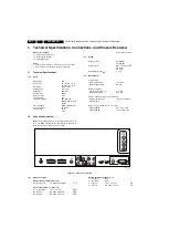
Page 2: ...A2 NICAM Sound effects SRS TrusurroundXT 3D Mono 3D Stereo Maximum power WRMS 2 12 1 1 3 Miscellaneous Power supply Mains voltage VAC 175 265 Mains frequency Hz 50 60 Ambient conditions Temperature range C 5 to 40 Maximum humidity 99 R H Power consumption values are indicative Normal operation W 155 32 229 42 Stand by W 1 Dimensions incl stand W H D in mm 32PFL2302 62 827 597 100 42PFL2302 62 1135...

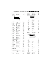
Page 3: ...nd H Cinch S PDIF Out Bk Coaxial 0 4 0 6VPP 75 ohm kq Cinch Video CVBS Out Audio Out Ye Video CVBS 1 VPP 75 ohm kq Wh Audio L 0 5 VRMS 10 kohm kq Rd Audio R 0 5 VRMS 10 kohm kq Cinch Video YPbPr In Audio In Gn Video Y 1 VPP 75 ohm jq Bu Video Pb 0 7 VPP 75 ohm jq Rd Video Pr 0 7 VPP 75 ohm jq Wh Audio L 0 5 VRMS 10 kohm jq Rd Audio R 0 5 VRMS 10 kohm jq HDMI Digital Video Digital Audio In Figure 1...

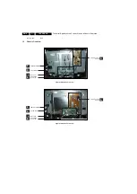
Page 4: ...assis Overview Figure 1 5 PWB locations 32 Figure 1 6 PWB locations 42 H_17490_012 eps 291007 LED PANEL A POWER SUPPLY BOARD B J SIDE I O PANEL D CONTROL BOARD E MAIN BOARD incl ext I O H_17490_014 eps 291007 LED PANEL A POWER SUPPLY BOARD B J SIDE I O PANEL D CONTROL BOARD E MAIN BOARD incl ext I O ...

Page 5: ...eforms and voltages with D and without E aerial signal Measure the voltages in the power supply section both in normal operation G and in stand by F These values are indicated by means of the appropriate symbols Manufactured under license from Dolby Laboratories Dolby Pro Logic and the double D symbol are trademarks of Dolby Laboratories 2 3 2 Schematic Notes All resistor values are in ohms and th...

Page 6: ... serial number Digits 1 and 2 refer to the production center e g AG is Bruges digit 3 refers to the B O M code digit 4 refers to the Service version change code digits 5 and 6 refer to the production year and digits 7 and 8 refer to production week in example below it is 2006 week 17 The 6 last digits contain the serial number Figure 2 1 Serial number example 2 3 6 Board Level Repair BLR or Compon...

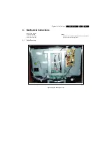
Page 7: ...ions Index of this chapter 4 1 Cable Dressing 4 2 Set Dis assembly 4 3 Set Re assembly Notes Figures below can deviate slightly from the actual situation due to the different set executions 4 1 Cable Dressing Figure 4 1 Cable Dressing 32 sets H_17490_011 eps 291007 ...

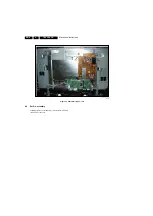
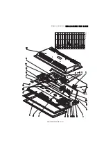
Page 8: ...Mechanical Instructions EN 8 TES2 0E LA 4 Figure 4 2 Cable Dressing 42 sets 4 2 Set Dis assembly Following figures exploded view indicate the mechanical construction of the sets H_17490_013 eps 291007 ...

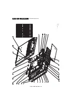
Page 9: ...Mechanical Instructions EN 9 TES2 0E LA 4 Figure 4 3 Exploded View 32 sets H_17490_015 eps 291007 ...

Page 10: ...Mechanical Instructions EN 10 TES2 0E LA 4 Figure 4 4 Exploded View 42 sets H_17490_016 eps 291007 ...

Page 11: ...Mechanical Instructions EN 11 TES2 0E LA 4 4 3 Set Re assembly Note While re assembling make sure that all cables are placed and connected in their original position See figures Cable dressing ...

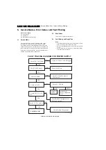
Page 12: ...hese sets do not generate Error Codes 5 3 Fault Finding and Repair Tips Notes It is assumed that the components are mounted correctly with correct values and no bad solder joints Before any fault finding actions check if the correct options are set The Service Menu see chapter 8 contains some useful tests that generates patterns Figure 5 1 Fault finding power supply FAULT TRACING DIAGRAM FOR POWER...

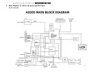
Page 13: ...Block Diagrams Test Point Overviews and Waveforms EN 13 TES2 0E LA 6 6 Block Diagrams Test Point Overviews and Waveforms Block Diagram Main H_17490_018 eps 291007 ...

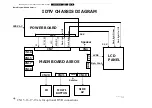
Page 14: ...V STD 12V Back light On Off Back light Dimm S300 CN7 IDTV CHASSIS DIAGRAM POWER BOARD MAIN BOARD ASSOS LCD PANEL SIDE AV MULTI BUTTON IR 24 V 24 V Back light Dimm Back light On Off 220 V AC CN17 CN16 CN15 CN19 J7 CN4 Speaker Service CN5 CN24 Dyn Cont LVDS CN15 16 17 19 are for optional DVB connections H_17490_019 eps 291007 ...

Page 15: ...Waveforms EN 15 TES2 0E LA 6 Block Diagram Board Location CN4 CN5 CN7 CN19 J7 CN18 CN22 CN16 CN17 CN21 CN20 CN15 J10 CN9 CN8 CN11 CN12 CN13 TUNER PC SOUND HDMI1 SCART1 SCART2 SPDIF OUT LINE OUT COMPONENT INPUT DVI HDMI2 H_17490_020 eps 291007 ...

Page 16: ...2 4V 1 1 2 2 3 3 4 4 5 5 6 6 IC41 TCDT1101G BL_ON OFF L402 10uH 7A 5VOC R336 1K 1 T400 BC848B R304 150K R414 1K R305 150K STB C414 2200uF 35V C409 47nF C408 100nF D404 MBR20200CT R412 10R R413 10R C416 1nF 1KV D315 12V C417 1nF 1KV C213 33uF 1 4 10 6 TR20 SMPS STANDBY LCD 24V C345 33pF 3 4 1 6 12 7 11 8 TR40 SMPS LCD BL A_DIM GND 1 GND 2 GND 3 VFB 4 VCC 5 VST 8 D 7 IC21 FSD200 R326 1K 5VMAIN D306 ...

Page 17: ...Circuit Diagrams and PWB Layouts EN 17 TES2 0E LA 7 Layout Power Supply Panel Top Side H_17490_022 eps 161007 Layout Power Supply Panel Top Side H_17490_023 eps 161007 ...

Page 18: ... A_GREEN A_BLUE A_HSYNC A_GND1 A_GND2 C4 100nF NU R19 0R C381 10pF R27 0R C12 10nF C17 10nF R561 0R R17 0R U5 24C02 5 6 8 4 1 2 3 7 SDA SCL VCC GND A0 A1 A2 WP C26 100nF R16 47K R466 1K C14 10nF R570 0 ED4 BAV99 NU 2 1 3 Q1 MMBT3904 1 3 2 R564 5 1K NU C18 10nF R566 5 1K NU C48 22pF NU C47 22pF NU Q30 MMBT3904 1 3 2 C29 100nF ED2 BAV99 NU 2 1 3 J1 PHONE_JACK 5 2 4 3 1 R2 R1 L2 L1 GND C44 22pF NU U2...

Page 19: ... 2 R409 270 R41 75_1 1 2 R37 75_1 1 2 FB61 600 Ohm 0 5A 2012 1 2 C387 22pF C465 22pF 1 2 CN15 JST250 4P 1 2 3 4 NC RXD_DVB TXD_DVB GND R35 0R NU 1 2 R415 82 C348 1nF C389 22pF R407 4 7K C453 10uF_2012 C42 1nF C50 220uF 16V C386 22pF FM1 Q25 MMBT3904 1 3 2 C463 22pF 1 2 R413 1M ED8 BAV99 2 1 3 C351 1nF FM2 R575 15K HH3 MTHOLE 1 2 3 4 5 6 7 8 9 R430 0R C454 10uF_2012 R417 470 R43 0R 1 2 R491 15K C34...

Page 20: ... 4 C90 100nF R436 22K C95 47nF R98 100R C458 100nF R92 470 C123 47nF TP23 R591 0R R121 47R C359 15nF R219 100R U9 DDR_128Mb_TSOP66 29 30 31 32 35 36 37 38 39 40 28 41 2 4 5 7 8 10 11 13 54 56 57 59 60 62 63 65 26 27 24 23 22 21 20 47 16 51 44 45 46 1 18 33 3 9 15 55 61 34 48 66 6 12 58 64 49 52 14 17 19 25 43 53 50 42 A0 A1 A2 A3 A4 A5 A6 A7 A8 A9 A10 AP A11 DQ0 DQ1 DQ2 DQ3 DQ4 DQ5 DQ6 DQ7 DQ8 DQ9...

Page 21: ...7 BAV99 2 1 3 R249 5 6K 1 2 R583 15K 1 2 R242 220K 1 2 J8B UJB0617D_RCA Triple_top NT NU 6 13 5 C143 NU 1 2 Q10 MMBT3904 1 3 2 R237 100 1 2 C132 47uF 25V 1 2 C134 10pF 1 2 R243 1M R582 15K 1 2 ED30 BAV99 NU 2 1 3 R238 220K 1 2 ED24 BAV99 NU 2 1 3 ED34 BAV99 2 1 3 C148 1nF J9C UJB0617D_RCA Triple_top NT NU 2 5 8 C137 1nF C142 1nF C149 1nF ED32 BAV99 2 1 3 R584 15K 1 2 C136 220uF 16V 1 2 ED38 BAV99 ...

Page 22: ...TXO3 4 TXO1 4 TXO1 4 TXO4 4 IR 4 LED_R 4 D_IR 3 LG_SEL_DCR 4 ODSEL1 4 RPForEXT_Vbr 4 PANEL_SYNC 4 ADC IN1 4 RPForEXT_Vbr 4 VSS3V VSS5 VSS3V 5VD 12VD VSS5 R605 0R R552 0R NU 1 2 JTP63 1 R269 150R 1 2 TP19 1 R611 0R NU R551 0R NU 1 2 R602 0R NU CN20 JST250 4P 1 2 3 4 5V_ST BY IR GND LED_ERD JTP82 1 JTP72 1 R270 1K 1 2 JTP70 1 R497 560 1 2 JTP79 1 R266 100R R594 0R 1 2 JTP68 1 JTP40 1 JTP77 1 FB7 UPB...

Page 23: ...DVSS PVSSR NC HP INL VREFL PVDDREG VSS SLEEPN PVSSL VSS OUTPL PVDDPL PVDDPL INR OUTPR PVDDPR VSS NC MUTEN PROTN OUTMR HPOL REFA PVDDMR NC VSSBGR GAIN1 NC VSS VREFR AVSS VSS PVDDPR PVDDMR VSS CKIO XO XI DVDD MODE0 MODE1 MODE2 GAIN0 VSS VSS TAP FB17 0_2012 1 2 R515 34 8K F R523 49 9K F R307 3 6K NU 1 2 C167 1 2nF R517 34 8K F C179 220uF 16V C450 10uF_2012 NU L12 22uH NU R538 0R NU R534 10K C445 470p...

Page 24: ...8 100nF R339 0R R333 1K FB27 600 Ohm 0 5A 2012 C199 4 7uF_2012 R329 1K C224 220uF 16V C218 100uF 16V 1 2 R360 75R C210 4 7uF_2012 C202 4 7uF_2012 FB28 600 Ohm 0 5A 2012 C230 100nF R308 1K U15 AZ78D05 1 2 3 4 INPUT GND OUTPUT TAP R343 1K R368 22K TP12 L13 0R_2012 C204 4 7uF_2012 R326 1K C225 100nF R338 1K R364 22K C238 1nF R365 220K 1 2 CN5 SMW250 4P NU 1 2 3 4 S5V GND RXD TXD R341 1K C207 4 7uF_20...

Page 25: ...209T 500Y S NU 2 1 C312 100nF C326 100nF CN11 SMW250 12P NU 1 2 3 4 5 6 7 8 9 10 11 12 5VSC 5VSC 5VSC GND GND GND 12VSC 12VSC GND GND NC NC C311 100nF R389 22 NU D12 NU FB30 UPB201209T 500Y S NU 2 1 C271 4 7uF 50V FB62 UPB201209T 500Y S NU FB31 UPB201209T 500Y S NU 2 1 Q20 MMBT3904 NU 1 3 2 C294 100nF U21 AP1117 2 5V_SOT223 3 1 2 4 VI GND VO TAP C305 100nF FB47 600 Ohm 0 5A 2012 C282 100nF FB33 UP...

Page 26: ...EN 26 TES2 0E LA 7 Circuit Diagrams and PWB Layouts Layout Main Board Top Side H_17490_009 eps 161007 ...

Page 27: ...2uH C100 220nF AGND C101 220nF AGND C102 100nF AGND C103 100nF AGND R100 4 7R C104 10nF AGND R101 4 7R C105 10nF AGND C100 47pF R104 75R 1 2 3 4 5 6 S106 S_VHS C101 47pF R105 75R AGND AGND AGND AGND AGND AGND AGND 7 8 1 5 4 3 2 S100 HEADPHONE 7P H_17490_024 eps 161007 D D SIDE I O PANEL Keyboard Control Panel 1 2 S001 To main pcb C001 100nF R002 2 2K 1 6W R003 330R 1 6W R004 3 3K 1 6W R005 6 8K 1 ...

Page 28: ...uts IR LED Panel 1 2 3 4 S001 INFRA RED R001 33R 1 4W C001 100uF GND R003 470R R004 15K 1 6W SW01 STBY 1 2 S002 To mbutton pcb C002 100nF IR 3 VCC 2 GND 1 IR01 IR LED1 LED J J H_17490_026 eps 161007 IR LED PANEL Personal Notes E_06532_012 eps 131004 ...

Page 29: ...gnments present in the sets 8 4 Software Alignments 8 4 1 Service Menu The Service Menu enables a large number of settings You can activate and deactivate options or change parameters that influence the quality of the displayed image Activate the Service Menu as follows Press the Menu button on the remote control the screen will display the Customer Menu Press 1923 on the remote control the screen...

Page 30: ...z I2C Integrated IC bus I F Intermediate Frequency LED Light Emitting Diode L L Monochrome TV system Sound carrier 6 5MHz France L is Band I L is all bands except for Band I LS Loudspeaker M N Monochrome TV system Sound carrier 4 5 MHz MCU Main Control Unit NC Not Connected NICAM Near Instantaneous Compounded Audio Multiplexing This is a digital sound system mainly used in Europe NTSC National Tel...

Page 31: ...ve Rx w EQ Rx w EQ Rx w EQ Rx w EQ VCC 3 3 V VCC VCC VCC VCC VCC VCC VCC 3 3 V V CC 3 3 V A11 B11 A12 B12 A13 B13 A14 B14 RINT RINT RINT RINT RINT RINT RINT R INT R INT R INT R INT RINT OE BLOCK DIAGRAM TMDS341A PIN CONFIGURATION HPD2 SDA2 SCL2 GND GND B21 A21 B22 A22 GND B23 A23 V B24 A24 GND HPD1 N C O E H P D 3 SD A 3 S C L3 GN D B 31 A 31 B 32 A 32 GN D B 33 A 33 B 34 A 34 GN D N C HPD_SINK SD...

Page 32: ...9 2 Internal block diagram and pin configuration PIN CONFIGURATION TS5V330 H_17490_028 eps 291007 D D DBQ OR PW PACKAGE TOP VIEW RGY PACKAGE TOP VIEW 1 16 8 9 2 3 4 5 6 7 15 14 13 12 11 10 EN S2D S2D DD S1C S2C S1A S2A DA S1B S2B DB IN V GND CC 1 2 3 4 5 6 7 8 16 15 14 13 12 11 10 9 IN S1A S2A DA S1B S2B DB GND VCC EN S1D S2D DD S1C S2C DC C ...

Page 33: ...119 120 121 123 125 127 122 124 126 128 MDATA 4 VDDM MDATA 3 MDATA 2 MDATA 1 MDATA 0 MVREF DQS 0 DQM MCLKF 180 179 176 175 172 170 168 166 165 163 161 159 157 154 152 150 178 177 174 173 171 169 167 164 162 160 158 156 155 153 151 149 148 147 146 145 143 142 141 144 DDCR_CK PWM1 SAR3 SAR1 SDO SDI SCK DDCR_DA PWM0 SAR2 SAR0 CSZ GND VDDP ALE RDZ WRZ AD 7 AD 6 AD 5 AD 4 AD 3 AD 2 AD 1 AD 0 MADR 11 MA...

Page 34: ...PA 27 PH3R 28 PH1L 29 PH2L 30 PH3L 31 GND 32 SCL 53 LHPB 52 LHP 51 VDA2 50 VSA2 49 VREF LMAXO 11 RMAXO 10 LVOLI 12 OUTPUTR 13 OUTPUTL 14 VDA1 15 VSA1 16 FSUMLRO 38 FMINRLO 39 FSUMI 37 VCC 36 A0 35 RSTB 34 SDA 33 BASSOUT PUNCHIN RVOLI COMPC MULTIN CLP COMPC2 FOUT CLPB 7 8 9 5 6 3 4 1 2 62 61 60 59 58 57 56 55 64 63 CB2B CB2 CB3B CB3 MIXOUT RHPA RHPB RHP CB1B CB1 54 LHPA 53 LHPB 52 LHP LMAXO 11 RMAX...

Page 35: ...0 20 19 18 17 16 15 14 13 24 23 22 21 11 12 GND CAPACITANCE L1 L2 L3 L4 L5 LOUT1 ROUT1 SDA SCL ADDR R1 R2 R3 R4 R5 VS L6 LOUT2 R6 ROUT3 LOUT3 ROUT2 1 2 3 4 5 6 7 8 9 10 20 19 18 17 16 15 24 23 22 21 11 12 25 13 14 28 27 26 SDA SCL ADDR R1 R2 R3 NC NC R4 R5 R6 ROUT3 LOUT3 ROUT2 LOUT2 ROUT1 LOUT1 L6 L5 L4 NC NC L3 L2 L1 GND CAPACITANCE VS SDIP24 SO28 RIGHT INPUTS GAIN 0 dB RIGHT OUTPUTS SDA SCL ADDR...

Page 36: ...BTD3306 U16 Figure 9 7 Internal block diagram and pin configuration PIN CONFIGURATION UDA1334BTS H_17490_032 eps 291007 UDA1334BTS 1 2 3 4 5 6 7 8 16 15 14 13 12 11 10 9 VOUTR BCK VSSA WS VOUTL DATAI VDDA VDDD Vref DAC VSSD SFOR0 SYSCLK PCS SFOR1 DEEM MUTE BLOCK DIAGRAM SN74CBTD3306 PIN CONFIGURATION H_17490_033 eps 291007 B 2 A 2 2OE 1A 1B 1OE 2 1 5 7 3 6 D OR PW PACKAGE TOP VIEW 1 2 3 4 8 7 6 5 ...

Page 37: ...block diagram and pin configuration 9 4 9 PWM Buck DC DC Converter AP1501 U26 Figure 9 9 Internal block diagram and pin configuration BLOCK DIAGRAM BA6161x PIN CONFIGURATION H_17490_034 eps 291007 PIN CONFIGURATION AP1501 H_17490_035 eps 291007 TO220 5L Top View Top View TO263 5L 1 V IN 5 SD 4 FB 3 Gnd 2 Output Metal Tab GND 1 V IN 5 SD 4 FB 3 Gnd 2 Output ...

Page 38: ...ons Abbreviation List and IC Data Sheets EN 38 TES2 0E LA 9 9 4 10 Audio Power Amplifier YDA143 U30 Figure 9 10 Internal block diagram and pin configuration PIN CONFIGURATION BLOCK DIAGRAM YDA143 H_17490_036 eps 291007 ...

Page 39: ...H32 LCD ID DVD WR TELRA CODE DESCRIPTION 005415025680 BACK COVER LABEL POLYE 82X263PH FTV 013466066231 LOGO PHILIPS PIMLI 62X12 5MM 065001045130 USER MANUELTV UYARI LCD PLAS RPT 065001046301 USER MANUELEK SYF LCD PLAS RPT 065001056950 USER MANUAL EASY26 32 PHILIPS TRK ING 065001066980 USER MANUELPHILIPS 32PFL2302 62 065011004232 Guarantee card PHILIPS 065011004620 Guarantee card PHI WORLDWIDECMB 0...

Page 40: ...Revision List EN 40 TES2 0E LA 11 11 Revision List 11 1 Manual xxxx xxx xxxxx 0 First release 11 2 Manual xxxx xxx xxxxx 1 Chapter 10 Spare part list added ...

Reviews: