Contents
Chapter
Adjustment Procedures
Schematic Diagrams and CBA's
Exploded Views
Mechanical and Electrical Parts Lists
Sec. 1:
Sec. 2: Standard Maintenance
Mechanism Alignment Procedures
Disassembly / Assembly of Mechanism
Deck Exploded Views
Deck Parts Lists
Survey of versions:
Published by FU-KC 0622 Service AV Systems Printed in The Netherlands Subject to modification
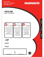
Version 1.0
/75 PAL
DVD + VCR Combi
DVP3200V
/75
c Copyright 2006 Philips Consumer Electronics B.V. Eindhoven, The Netherlands
All rights reserved. No part of this publication may be reproduced, stored in a retrieval
system or transmitted, in any form or by any means, electronic, mechanical, photocopying,
or otherwise without the prior permission of Philips.
CLASS 1 LASER PRODUCT
KLASSE 1 LASER PRODUKT
KLASS 1 LASER APPARAT
CLASSE 1 PRODUIT LASER
GB 3139 785 32020
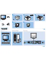
STOP
PLAY
REW
F.FWD
PLAY
REC
CHANNEL
STOP/EJECT
VIDEO
AUDIO
L
R
SOURCE
STANDBY-ON
VCR
DVD
DVD
OPEN/CLOSE
Service Manual
Service
Service
Service
Service
Service