background image

http://servis-manual.com/

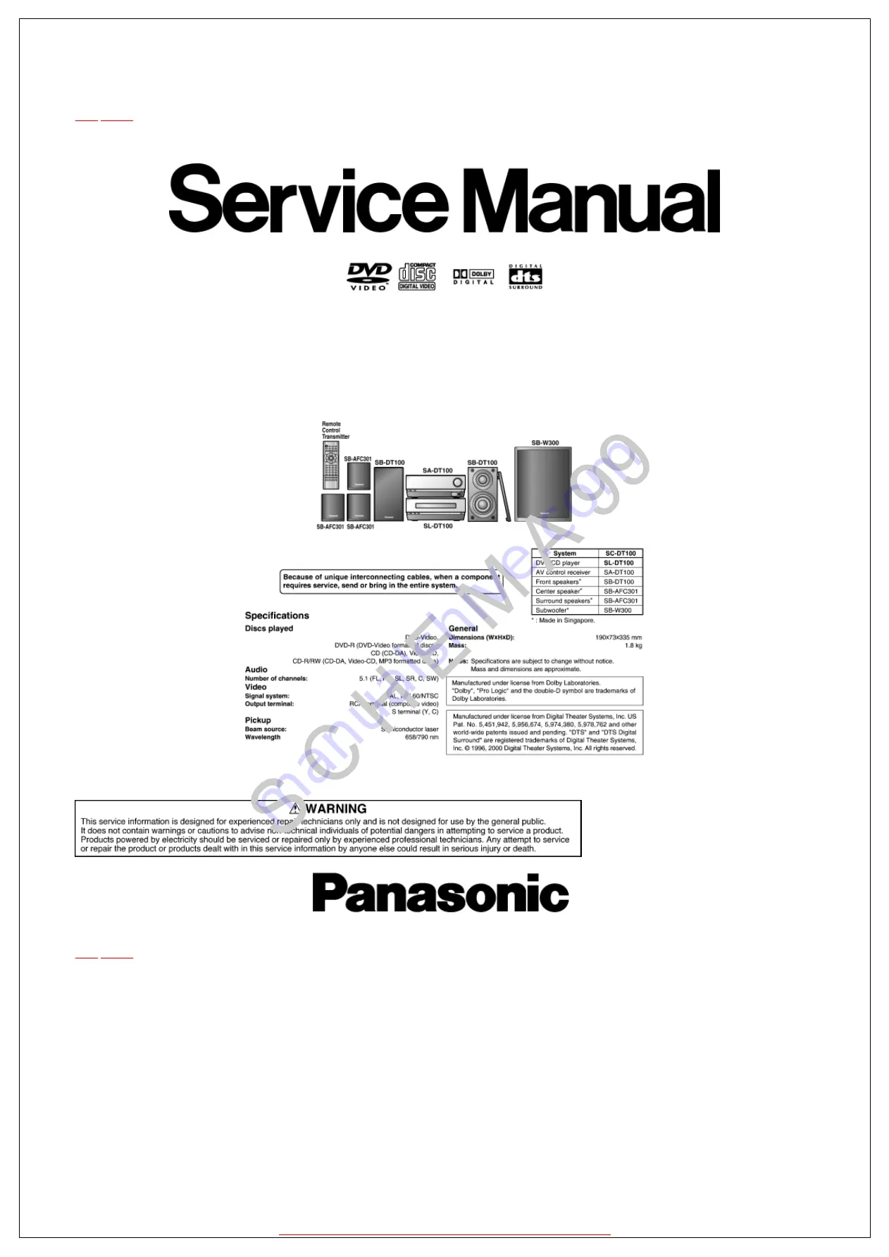
Service Manual 

TOP


NEXT


AD0203069C2 


DVD/CD Player  


l

SL-DT100EG 

Traverse Deck: RAE1813Z Mechanism Series 

Colour 

(S)...........Silver Type 


© 2002 Matsushita Electric Industrial Co., Ltd. All rights reserved. Unauthorized copying and distribution is a violation of law. 


TOP


NEXT
  

Summary of Contents for SL-DT100EG

Page 1: ...TOP NEXT AD0203069C2 DVD CD Player l SL DT100EG Traverse Deck RAE1813Z Mechanism Series Colour S Silver Type 2002 Matsushita Electric Industrial Co Ltd All rights reserved Unauthorized copying and distribution is a violation of law TOP NEXT ...

Page 2: ...rently in use Our new DVD player Remarks UHF error display The latest error storage n 1 UHF error display The latest error storage n 20 The storage capacity is increased Jitter read error display Jitter read error display Focus drive value display The focus drive current value can be displayed Laser drive current display for DVD Laser drive current display for DVD CD ADSC internal RAM data display...

Page 3: ...asurement The value denotes the current in decimal notation The above example shows the initial current is 34 mA and 28 mA for DVD and CD laser Cancelled automatically 5 seconds later DVD laser drive current measure ment In STOP mode press STOP button on the player and OSD button on the remote control unit DVD laser drive current measurement DVD laser drive current is measured and the result is di...

Page 4: ...e version Cancelled automatically 5 seconds later Timer 1 check In STOP mode press STOP button on the player and button on the remote control unit Timer 1 check Laser operation timer Operation time is measured separately for DVD and CD laser T1_1234_5678 Shown to the left is DVD laser time and to the right is CD laser time Time is shown in 4 digits of decimal notation in a unit of 10 hours 0000 wi...

Page 5: ...ODC ODC related F600 Access failure to management information caused by demodulation error Operation stopped because navigation data is not accessible caused by the demodulation defect ODC FEP ADSC F601 Indeterminate sector ID requested Operation stopped caused by the request to access abnormal ID data ODC FEP ADSC F602 Access failure to LEAD IN caused by demodulation error LEAD IN data unreadable...

Page 6: ...rrect firmware bug Firmware bug F890 Sending message when message is being sent to AV task Sending message to AV task Stop the operation by error need to correct firmware bug Firmware bug F891 Message could not be sent to AV task Begin sending message to AV task Stop the operation by error need to correct firmware bug Firmware bug F893 FROM falsification FROM CPU F894 EEPROM abnormality EEPROM Ser...

Page 7: ...ton to select DVD 3 With no disc on the unit hold down STOP button for at least 2 seconds and then press button for at least 2 seconds 4 A loading mechanism error code is displayed if any Refer to Table 5 1 If there are multiple error they can be successively by pressing STOP button TOP PREVIOUS NEXT ...

Page 8: ...tion TOP PREVIOUS NEXT l Press the Standby on button to turn off And then press the Standby on button again to turn it on again l The contents of self diagnosis function are stored in memory To re display perform the procedures How to display TOP PREVIOUS NEXT ...

Page 9: ... is displayed on the LCD about 2 seconds Clearing the contents of self diagnosis function l Always be sure to clear memories after completing repair TOP PREVIOUS NEXT Table 5 1 Display code Symptom Cause H15 When the disc tray opens it closes by itself Disc tray open close detect switch S1001 fault Check and replace H16 When the disc tray closes it opens by itself ...

Page 10: ...t DVD Video Audio VR PCND_NOPLAY VIDEO 0x70 DiscManager 0xD0C0 F0C1 9 DVD Prohibited by the restricted region code PCND_NOPLAY RCD 0x80 DiscManager 0xD0C1 F0C2 A DVD PAL restricted playback PCND_NOPLAY PAL 0x90 DiscManager 0xD0C2 F0C3 B DVD Parental lock setting prohibits the playback of the entire title PCND_NOPLAY PTL 0xA0 DiscManager 0xD0C3 F0C4 C VCD Prohibited because it is in PHOTO CD format...

Page 11: ... DVD D L1 4B6 Focus balance learning value for DVD S DVD D L0 CD and VCD 4BE Focus balance learning value for DVD D L1 4B5 Tracking gain learning value for DVD S DVD D L0 CD and VCD 4BD Tracking gain learning value for DVD D L1 TB0 Tracking balance learning value for DVD S DVD D L0 CD and VCD TB1 Tracking balance learning value for DVD D L1 DBD DSL offset learning value for DVD S and DVD D DBC DSL...

Page 12: ...ng procedures after completing repairs 1 Close the disc tray to press button 2 Turn off the power to press Standby on button 3 Disconnect an AC cord from the outlet Note Do not disconnect an AC cord from the outlet with the disc tray is still opens then close the disc tray manually TOP PREVIOUS NEXT ...

Page 13: ...f diagnosis and tilt adjustment Be sure to use the self diagnosis functionbefore replacing the optical pick up when NO DISC is displayed As a guideline you should replace the optical pick up when the value of the laser drive current is more than 70 DVD 55 CD Note Press the Standby on button to turn on the power and check the value within three minutes before the unit warms up Otherwise the unit wi...

Page 14: ... button on the remote control unit while pressing the STOP button on the player T1_xxxx_yyyy xxxx DVD yyyy CD Time is shown in 4 digits of decimal notation in a unit of 10 hours Using hours of spindle motor Press button on the remote control unit while pressing the STOP button on the player T2_xxxx xxxx Time is shown in 4 digits of decimal notation in a unit of 10 hours Resetting using hours of DV...

Page 15: ...andling Precaution for TraverseDeck l Do not touch the area around the laser diode and actuator l Do not judge the laser diode with a tester l It is recommended to use an antistatic soldering iron for short circuit or removing the laser diode Recommended soldering iron HAKKO ESD Product l Solder the land of the flexible cable in the optical pick up Note When using a soldering iron which is not ant...

Page 16: ...ber which noted at the connectors on the schematic diagram as SCHEMATIC DIAGRAM 1 or SCHEMATIC DIAGRAM 2 indicates the schematic diagram serial number located on the left corner in the schematic diagram SL DT100 EG TERMINAL SERVO CIRCUIT DIAGRAM 37 36 35 34 38 33 32 31 30 29 28 27 26 25 24 23 22 21 20 19 18 17 16 15 14 13 12 11 10 9 8 7 6 5 4 3 1 2 POSITIVE VOLTAGE LINE VIDEO AUDIO SIGNAL LINE ...

Page 17: ...ber which noted at the connectors on the schematic diagram as SCHEMATIC DIAGRAM 1 or SCHEMATIC DIAGRAM 2 indicates the schematic diagram serial number located on the left corner in the schematic diagram SL DT100 EG TERMINAL SERVO CIRCUIT DIAGRAM 37 36 35 34 38 33 32 31 30 29 28 27 26 25 24 23 22 21 20 19 18 17 16 15 14 13 12 11 10 9 8 7 6 5 4 3 1 2 POSITIVE VOLTAGE LINE VIDEO AUDIO SIGNAL LINE ...

Page 18: ...22K Q5211 2SB1115 T LASER POWER DRIVE DVD C5215 6 3V47 R5215 2 2 R5216 27 R5217 47K Q5215 2SB1115 T LASER POWER DRIVE CD A1 A2 A3 A4 A5 A6 A7 C1 C3 C4 C5 C6 C7 C8 C9 C10 C11 C12 C12 TBAL FS14 FBAL FS15 DTRD FS16 IDGT FS17 FEPENB FS19 FEPCLK FS20 FEPDATA FS21 JLINE FS22 TE FS23 AS FS24 FE FS25 C11 C10 C9 C8 C7 C6 C4 C3 C2 C1 SAGCAN FC2 A 5V AB1 A GND AG1 C5201 16V10 C5203 0 1 L5201 ELJEA100KF RFENV...

Page 19: ...22K Q5211 2SB1115 T LASER POWER DRIVE DVD C5215 6 3V47 R5215 2 2 R5216 27 R5217 47K Q5215 2SB1115 T LASER POWER DRIVE CD A1 A2 A3 A4 A5 A6 A7 C1 C3 C4 C5 C6 C7 C8 C9 C10 C11 C12 C12 TBAL FS14 FBAL FS15 DTRD FS16 IDGT FS17 FEPENB FS19 FEPCLK FS20 FEPDATA FS21 JLINE FS22 TE FS23 AS FS24 FE FS25 C11 C10 C9 C8 C7 C6 C4 C3 C2 C1 SAGCAN FC2 A 5V AB1 A GND AG1 C5201 16V10 C5203 0 1 L5201 ELJEA100KF RFENV...

Page 20: ... MUTE3 28 LDCNT ACT T FS4 ACT F FS2 ACT F FS3 ACT T FS1 L2501 0 C2502 6 3V330 C2505 0 1 TRVS FS11 TRVS FS12 DM FS9 DM FS10 R2504 100 TRAYMUT SA5 TRAYREF SA3 C2512 0 1 TRAYDRV SA4 TRAY TRV SA2 M 9V MB1 C2501 6 3V100 C2503 16V100 C2504 0 1 C2507 0 1 M GND MG1 R2505 100 IC2501 C0GBG0000020 STEPPING MOTOR FOCUS TRACKING COIL DRIVE C2506 0 1 C2508 0 1 D 5V DB3 VHALF FS32 VREF2 FS33 C2053 0 1 A 5V AB1 R...

Page 21: ... MUTE3 28 LDCNT ACT T FS4 ACT F FS2 ACT F FS3 ACT T FS1 L2501 0 C2502 6 3V330 C2505 0 1 TRVS FS11 TRVS FS12 DM FS9 DM FS10 R2504 100 TRAYMUT SA5 TRAYREF SA3 C2512 0 1 TRAYDRV SA4 TRAY TRV SA2 M 9V MB1 C2501 6 3V100 C2503 16V100 C2504 0 1 C2507 0 1 M GND MG1 R2505 100 IC2501 C0GBG0000020 STEPPING MOTOR FOCUS TRACKING COIL DRIVE C2506 0 1 C2508 0 1 D 5V DB3 VHALF FS32 VREF2 FS33 C2053 0 1 A 5V AB1 R...

Page 22: ...00063 MEMORY 28 VSS 27 VDD 29 A4 30 A5 31 A6 32 A7 33 A8 34 A9 35 A11 36 NC 37 CKE 38 CLK 39 UDQM 40 NC 41 VSS 42 DQ8 43 VDDQ 44 DQ9 45 DQ10 46 VSSQ 47 DQ11 48 DQ12 49 VDDQ 50 DQ13 51 DQ14 52 VSSQ 53 DQ15 54 VSS 26 A3 25 A2 24 A1 23 A0 22 A10 AP 21 BA1 20 BA0 19 CS 18 RAS 17 CAS 16 WE 15 LDQM 14 VDD 13 DQ7 12 VSSQ 11 DQ6 10 DQ5 9 VDDQ 8 DQ4 7 DQ3 6 VSSQ 5 DQ2 4 DQ1 3 VDDQ 2 DQ0 1 VDD BA1 LDQM WE C...

Page 23: ...00063 MEMORY 28 VSS 27 VDD 29 A4 30 A5 31 A6 32 A7 33 A8 34 A9 35 A11 36 NC 37 CKE 38 CLK 39 UDQM 40 NC 41 VSS 42 DQ8 43 VDDQ 44 DQ9 45 DQ10 46 VSSQ 47 DQ11 48 DQ12 49 VDDQ 50 DQ13 51 DQ14 52 VSSQ 53 DQ15 54 VSS 26 A3 25 A2 24 A1 23 A0 22 A10 AP 21 BA1 20 BA0 19 CS 18 RAS 17 CAS 16 WE 15 LDQM 14 VDD 13 DQ7 12 VSSQ 11 DQ6 10 DQ5 9 VDDQ 8 DQ4 7 DQ3 6 VSSQ 5 DQ2 4 DQ1 3 VDDQ 2 DQ0 1 VDD BA1 LDQM WE C...

Page 24: ...1 H B To DVD MODULE AVDEC CIRCUIT on SCHEMATIC DIAGRAM 4 1 H B To DVD MODULE AUDIO DAC CIRCUIT on SCHEMATIC DIAGRAM 6 1 B B To DVD MODULE CPU CIRCUIT on SCHEMATIC DIAGRAM 7 12 H B To DVD MODULE CPU CIRCUIT on SCHEMATIC DIAGRAM 7 1 A B To DVD MODULE SODC CIRCUIT on SCHEMATIC DIAGRAM 3 12 E B To DVD MODULE SODC CIRCUIT on SCHEMATIC DIAGRAM 3 12 C B To DVD MODULE CPU CIRCUIT on SCHEMATIC DIAGRAM 7 1 ...

Page 25: ...1 H B To DVD MODULE AVDEC CIRCUIT on SCHEMATIC DIAGRAM 4 1 H B To DVD MODULE AUDIO DAC CIRCUIT on SCHEMATIC DIAGRAM 6 1 B B To DVD MODULE CPU CIRCUIT on SCHEMATIC DIAGRAM 7 12 H B To DVD MODULE CPU CIRCUIT on SCHEMATIC DIAGRAM 7 1 A B To DVD MODULE SODC CIRCUIT on SCHEMATIC DIAGRAM 3 12 E B To DVD MODULE SODC CIRCUIT on SCHEMATIC DIAGRAM 3 12 C B To DVD MODULE CPU CIRCUIT on SCHEMATIC DIAGRAM 7 1 ...

Page 26: ... R6513 10K R6514 47 LB6513 VLP0155 T X6501 VSX1044 36 864MHz C6512 15P C6511 15P R6512 330 3 GND 2 INA 1 N C 4 OUTY 5 VCC IC6521 C0JBAB000356 NOT GATE C6521 0 1 LB6521 VLP0323A601R D GND DG1 R6515 10 CLK33M AC7 CLKSEL AC8 CLK16M SA1 EXTCLK AD1 LB6522 VLP0155 T C4221 0 1 C4222 0 1 C4223 0 1 C4224 0 1 C4225 0 1 C4226 0 1 C4227 0 1 AC3H AC5 AMUT AC6 VLP0323A601R VLP0323A601R VLP0323A601R VLP0323A601R...

Page 27: ... R6513 10K R6514 47 LB6513 VLP0155 T X6501 VSX1044 36 864MHz C6512 15P C6511 15P R6512 330 3 GND 2 INA 1 N C 4 OUTY 5 VCC IC6521 C0JBAB000356 NOT GATE C6521 0 1 LB6521 VLP0323A601R D GND DG1 R6515 10 CLK33M AC7 CLKSEL AC8 CLK16M SA1 EXTCLK AD1 LB6522 VLP0155 T C4221 0 1 C4222 0 1 C4223 0 1 C4224 0 1 C4225 0 1 C4226 0 1 C4227 0 1 AC3H AC5 AMUT AC6 VLP0323A601R VLP0323A601R VLP0323A601R VLP0323A601R...

Page 28: ...A2 78 NIRQ3 PA3 79 NIRQ4 PA4 80 ADSEP 81 NRST 82 V DD 83 D0 84 D1 85 D2 86 D3 87 D4 88 D5 89 D6 90 D7 91 V SS 92 D8 93 D9 94 D10 95 D11 96 D12 97 D13 98 D14 99 D15 100 8 VCC A0 1 A1 2 A2 3 GND 4 7 WP 6 SCL 5 SDA C6221 0 1 IC6221 C3EBFC000025 EE PROM LB6221 VLP0323A601R C6223 0 1 IC6223 C0JBAA000001 AND GATE C6222 0 1 GND 3 INA 2 INB 1 4 OUTY 5 VCC IC6222 C0JBAA000001 AND GATE GND 3 INA 2 INB 1 4 O...

Page 29: ...A2 78 NIRQ3 PA3 79 NIRQ4 PA4 80 ADSEP 81 NRST 82 V DD 83 D0 84 D1 85 D2 86 D3 87 D4 88 D5 89 D6 90 D7 91 V SS 92 D8 93 D9 94 D10 95 D11 96 D12 97 D13 98 D14 99 D15 100 8 VCC A0 1 A1 2 A2 3 GND 4 7 WP 6 SCL 5 SDA C6221 0 1 IC6221 C3EBFC000025 EE PROM LB6221 VLP0323A601R C6223 0 1 IC6223 C0JBAA000001 AND GATE C6222 0 1 GND 3 INA 2 INB 1 4 OUTY 5 VCC IC6222 C0JBAA000001 AND GATE GND 3 INA 2 INB 1 4 O...

Page 30: ...417 4 7K R418 4 7K R405 47K R416 4 7K R411 4 7K R402 1K C402 100P Q402 2SD1819ATX INTERFACE Q401 2SD1819ATX INTERFACE Q403 2SD1819ATX INTERFACE R426 4 7K R456 100 R436 82K R457 100 D404 MA111TX C404 0 1 R428 47K R415 22K D401 MA111TX R406 1K R413 47K R430 4 7K F E G A C B E D IC501 C9ZB00000394 8bit MICRO CONTROLLER IC805 NJM4580EDTE1 MIXING AMP 4 3 2 1 8 7 6 5 R869 10K R870 10K C851 6 3V47 R866 1...

Page 31: ...417 4 7K R418 4 7K R405 47K R416 4 7K R411 4 7K R402 1K C402 100P Q402 2SD1819ATX INTERFACE Q401 2SD1819ATX INTERFACE Q403 2SD1819ATX INTERFACE R426 4 7K R456 100 R436 82K R457 100 D404 MA111TX C404 0 1 R428 47K R415 22K D401 MA111TX R406 1K R413 47K R430 4 7K F E G A C B E D IC501 C9ZB00000394 8bit MICRO CONTROLLER IC805 NJM4580EDTE1 MIXING AMP 4 3 2 1 8 7 6 5 R869 10K R870 10K C851 6 3V47 R866 1...

Page 32: ...OUT GND V IN IC5 NJM78M05FA REGULATOR IC2 C0DBZHE00011 REGULATOR Q3 2SB766ATX REGULATOR C19 1000P Q2 FMW1T98 STABILIZER R12 470 D12 MA111TX C18 16V10 R9 1 2K D11 MA111TX R8 22K R11 100 3 2 1 4 5 V IN VC VO NC GND K C16 1000P C17 16V47 R6 1K R17 10 D10 MA8082MTX I G O V OUT GND V IN IC6 C0CAAHF00001 REGULATOR 3 2 1 4 5 V IN VC VO NC GND 3 2 1 4 5 V IN VC VO NC GND C20 16V10 L4 C23 6 3V820 R14 2 2K ...

Page 33: ...OUT GND V IN IC5 NJM78M05FA REGULATOR IC2 C0DBZHE00011 REGULATOR Q3 2SB766ATX REGULATOR C19 1000P Q2 FMW1T98 STABILIZER R12 470 D12 MA111TX C18 16V10 R9 1 2K D11 MA111TX R8 22K R11 100 3 2 1 4 5 V IN VC VO NC GND K C16 1000P C17 16V47 R6 1K R17 10 D10 MA8082MTX I G O V OUT GND V IN IC6 C0CAAHF00001 REGULATOR 3 2 1 4 5 V IN VC VO NC GND 3 2 1 4 5 V IN VC VO NC GND C20 16V10 L4 C23 6 3V820 R14 2 2K ...

Page 34: ...both of the above operations are automatically performed Commercially available CD R can now perform updating and recovery process making it easier to update the version Recovery process Optimization of player after replacement of FROM EEPROM and module P C B Version updating Firmware updating for improved operability and performance TOP PREVIOUS NEXT ...

Page 35: ...st errors storage 1 event 20 events Utilization of the above functions in combination with servicing procedures is expected to contribute to higher efficiency of fault diagnosis Purposes Operation time display function For fault finding of spindle motor or laser that has limited service life ADSC internal RAM display function For faulty part identification in servo system using the learned values ...

Page 36: ...http servis manual com ...

Reviews: