


file:///E:/PV-9661_PV-9662/SVC/s0000000000.html
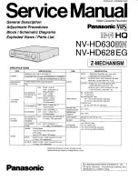
Service Manual
ORDER NO. MKE9901002C1
B3
Video Cassette Recorder
●
PV-9661/PV-9662
© 1999 Matsushita-Kotobuki Electronics Industries LTD. All rights reserved. Unauthorized copying and distribution is a
violation of law.
file:///E:/PV-9661_PV-9662/SVC/s0000000000.html (1 z 2) [2006-01-28 11:08:20]
Summary of Contents for Omnivision PV-9661
Page 272: ...5 2 MECHANISM SECTION 5 2 1 Disassembly Method Fig J1 1 23 PV 9661 PV 9662...
Page 273: ...5 2 2 EJECT Position Confirmation Fig J1 2 24 PV 9661 PV 9662...
Page 284: ...6 ADJUSTMENT PROCEDURES 6 1 SERVICE FIXTURES AND TOOLS 35 PV 9661 PV 9662...
Page 291: ...6 4 TEST POINTS AND CONTROL LOCATION 42 PV 9661 PV 9662...
Page 311: ...PV 9661 PV 9662 62...
Page 330: ...10 EXPLODED VIEWS 10 1 MECHANISM TOP SECTION 81 PV 9661 PV 9662...
Page 331: ...10 2 MECHANISM BOTTOM SECTION 82 PV 9661 PV 9662...
Page 332: ...10 3 CASSETTE UP COMPARTMENT SECTION 83 PV 9661 PV 9662...
Page 333: ...10 4 CHASSIS FRAME AND CASING PARTS SECTION 84 PV 9661 PV 9662...
Page 334: ...10 5 PACKING PARTS AND ACCESSORIES SECTION 85 PV 9661 PV 9662...