background image

ORDER NO. KM40208935C3

Telephone Equipment

KX-TMC40JX-W

Telephone Answering System

White Version

(for Asia, Middle Near East and other areas)

SPECIFICATIONS

Summary of Contents for KX-TMC40JX-W

Page 1: ...ORDER NO KM40208935C3 Telephone Equipment KX TMC40JX W Telephone Answering System White Version for Asia Middle Near East and other areas SPECIFICATIONS ...

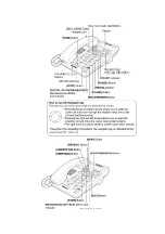
Page 2: ...2002 Kyushu Matsushita Electric Co Ltd All rights reserved Unauthorized copying and distribution is a violation of law 1 LOCATION OF CONTROLS ...

Page 3: ......

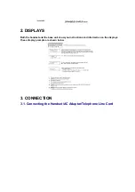
Page 4: ...ISPLAYS Both the handset and the base unit show you instructions and information on the displays These display prompts are shown below 3 CONNECTION 3 1 Connecting the Handset AC Adaptor Telephone Line Cord ...

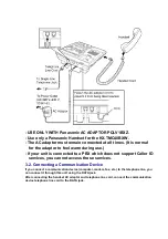
Page 5: ...t is connected to a PBX which does not support Caller ID services you cannot access those services 3 2 Connecting a Communication Device If you connect a communication device computer modem fax etc to the telephone line you can connect it through this unit using the DATA jack After connecting the handset AC adaptor and telephone line cord connect the communication device telephone line cord to the...

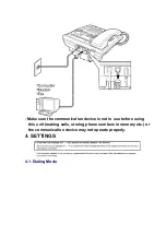
Page 6: ... Make sure the communication device is not in use before using this unit making calls storing phone numbers in memory etc or the communication device may not operate properly 4 SETTINGS 4 1 Dialing Mode ...

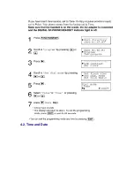
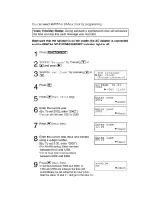
Page 7: ...4 2 Time and Date ...

Page 8: ......

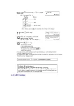
Page 9: ...4 3 LCD Contrast ...

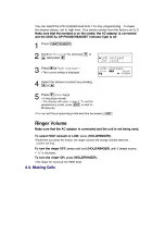
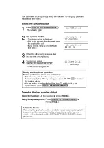
Page 10: ...4 4 Making Calls ...

Page 11: ......

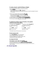
Page 12: ...4 5 Answering Calls ...

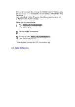
Page 13: ...4 6 Caller ID Service ...

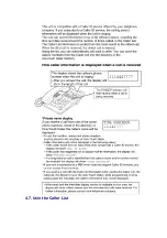
Page 14: ...4 7 Usin the Caller List ...

Page 15: ...4 8 Viewing the Caller List ...

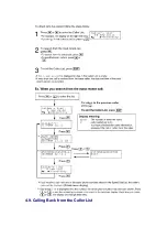
Page 16: ...4 9 Calling Back from the Caller List ...

Page 17: ...4 10 Dial Lock 4 10 1 To cancel the dial lock Follow above steps 1 through 3 In step 3 will go out 4 11 How to Release the Establishment of Dial Lock ...

Page 18: ...4 12 FLASH Button ...

Page 19: ...Note for Service When there is no battery a Flash function may not operate appropriately 5 DISASSEMBLY INSTRUCTIONS ...

Page 20: ...Shown in Fig To Remove Remove 1 Lower Cabinet Screws 2 6 X 12 A X 5 2 Main P C Board The Main P C Board 3 Operational P C Board Screws 2 6 X 8 B X 6 6 TROUBLESHOOTING GUIDE ...

Page 21: ...Check Power Error Message Table Check Playback Check Record Check Sp phone Voice Transmission Check Sp phone Voice Reception Check Handset Voice Transmission Check Handset Voice Reception Check Call ID 6 1 Check Power ...

Page 22: ...Cross Reference Power Supply Circuit Initializing Circuit NOTE Flash Memory are IC300 and IC306 DSP is IC201 6 2 Error Message Table NOTE Flash Memory are IC300 and IC306 DSP is IC201 ...

Page 23: ...6 3 Check Record Cross Reference Greeting Recording Circuit Telephone Line Interface ICM Recording Circuit NOTE Flash Memory are IC300 and IC306 DSP is IC201 6 4 Check Playback ...

Page 24: ...t NOTE Flash Memory are IC300 and IC306 DSP is IC201 6 5 Check Sp phone Voice Transmission Cross Reference SP PHONE TX Circuit Telephone Line Interface NOTE Flash Memory are IC300 and IC306 DSP is IC201 6 6 Check Sp phone Voice Reception ...

Page 25: ...ONE RX Circuit NOTE Flash Memory are IC300 and IC306 DSP is IC201 6 7 Check Handset Voice Transmission Cross Reference Handset TX Circuit Telephone Line Interface NOTE Flash Memory are IC300 and IC306 DSP is IC201 6 8 Check Handset Voice Reception ...

Page 26: ...ce Telephone Line Interface Handset RX Circuit NOTE Flash Memory are IC300 and IC306 DSP is IC201 6 9 Check Call ID Cross Reference Calling Line Identification Circuit Caller ID NOTE Flash Memory are IC300 and IC306 ...

Page 27: ...DSP is IC201 7 TEST MODE 8 BLOCK DIAGRAM 9 CIRCUIT OPERATION 9 1 SP PHONE RX Circuit Circuit Operation Telephone Line T R Q106 R160 R161 C160 pin 36 of IC201 pins 29 and 31 of IC201 Speaker ...

Page 28: ...9 2 SP PHONE TX Circuit Circuit Operation MIC C403 R403 C404 R404 pins 46 and 47 of IC201 pins 34 of IC201 R152 C151 R151 Q106 Telephone Line ...

Page 29: ...eceiving status or OGM transmitting status Circuit Operation The voltage pin 35 of IC201 is monitored If a parallel connected telephone is put into an OFF HOOK status the presence absence of a parallel connection is determined when the voltage changes by 0 2V or more When the set detects the parallel connected telephone is OFF HOOK status the line is disconnected ...

Page 30: ...3 The voltage at point B is dropped by D303 and L301 to 3 3V The voltage at point C is dropped by D304 to 3 3V The voltage at point D is dropped by D305 to 3 3V 9 5 DTMF Signal When the DTMF data from the Handset is received the DTMF signal is output from pin 34 of IC201 and sent to the line through Q106 9 6 Handset TX Circuit MIC C411 R411 R412 C413 Q410 C414 44 pin of IC201 34 pin of IC201 R152 ...

Page 31: ...9 7 Handset RX Circuit T R Q106 R160 R161 C610 36 pin of IC201 33 pin of IC201 C421 R422 R427 Q422 C426 SP ...

Page 32: ...data for the caller ID from the telephone exchange is sent during the interval between the first and second rings of the bell signal The data from the telephone exchange is a modem signal which is modulated in an FSK Frequency Shift Keying format Data 0 is a 1200 Hz sine wave and data 1 a 2200 Hz sine wave There are two type of the message format which can be received i e the single message format...

Page 33: ... he she can use this information to decide whether to take the new call Function The CAS signal flows from T R C181 C182 R181 R182 IC201 pins 38 40 and the ACK DTMFsignal is returned to the telephone exchange The telephone exchange that received the ACK can send the data in the same manner as the callerID If the unit deems that a telephone connected in parallel is in use ACK is not returned even i...

Page 34: ...hook or off hook by detecting changes in the T R voltage Circuit Operation Parallel connection detection when on hook When on hook Q101 is ON the voltage is monitored pin 35 of IC201 There is no parallel connection if the voltage is 1 65 V or higher while a parallel connection is deemed to exist if the voltage is lower Parallel connection detection when off hook When off hook Q101 is OFF the volta...

Page 35: ...tivation and control of at that functions such as speech Recording Playback Tone detecting and Line momitoring The DSP system comprises of following a Host Processor a Digital Signal Processor which includes the Firmware implemented functions a FLASH MEMORYS IC300 IC306 which is used for stored voice messages and synthesized voice Voice Message Recording Play back The DSP system use a proprietary ...

Page 36: ... built in speech detector and an FLASH MEMORYS IC300 IC306 which stored the vocabulary Caller ID and Call Waiting CID demodulation The DSP implements monitor and demodulate the FSK signals that provide CID information from the Central Office 9 11 Greeting Recording Circuit Circuit Operation MIC C403 C404 R403 R404 pins 46 and 47 of IC201 9 12 Greetin Play Back Circuit Circuit Operation Pin 34 of I...

Page 37: ...9 13 ICM Recording Circuit Circuit Operation Telephone Line C109 R160 R161 C160 pin 36 of IC201 ...

Page 38: ...Play Circuit Circuit Operation Pins 29 and 31 of IC201 Speaker 9 15 Telephone Line Interface Circuit Operation ANSWER In the idle mode Q103 is open to cut the DC loop current and decrease the ring load When ring ...

Page 39: ...ected as to cut the DC loop current and to cut the voice signal The unit is consequently in an on hook condition SPECIFICATIONS In the on hook state idle the current flows between the telephone line and the unit is as follows T L101 R2 C2 R4 C3 R2 L102 R The DC component is blocked by C2 C3 thereby providing an on hook condition The AC interface impedance is over 100k thus satisfying the telephone...

Page 40: ...10 CPU DATA 10 1 IC201 ...

Page 41: ...11 FLASH MEMORY 11 1 IC300 IC301 ...

Page 42: ...12 MODULE BLOCK DIAGRAM 12 1 LCD MODULE BLOCK ...

Page 43: ...E Enable Signal H 9 D C Data Command Control H L 10 CS Chip Signal L 11 RES Reset Signal Input L 13 HOW TO REPLACE FLAT PACKAGE IC 13 1 Preparation SOLDER Sparkle Solder 115A 1 115B 1 or Almit Solder KR 19 KR 19RMA Soldering iron Recommended power consumption will be between 30 W to 40 W Temperature of Copper Rod 662 50 F 350 10 C An expert may handle between 60 W to 80 W iron but beginner might d...

Page 44: ...t matter is accurate setting of IC to the corresponding soldering foil 2 Apply flux for all pins of FLAT PACKAGE IC 3 Solder employing specified solder to direction of arrow as sliding the soldering iron 13 3 Modification Procedure of Bridge 1 Re solder slightly on bridged portion 2 Remove remained solder along pins employing soldering iron as shown in below figure ...

Page 45: ...14 TERMINAL GUIDE OF ICs TRANSISTORS AND DIODES 15 CABINET AND ELECTRICAL PARTS ...

Page 46: ...16 ACCESSORIES AND PACKING MATERIALS ...

Page 47: ...availability is depends on the type of assembly and in accordance with the laws governing parts and product retention After end of this period the assembly will no longer be available 2 Important safety notice Components identified by mark have special characteristics important for safety When replacing any of these components use only manufacture s specified parts 3 The S mark means the part is o...

Page 48: ...ks 1 PQAS57P03Y SPEAKER 2 PQBC10347Z1 PUSH BUTTON SP PHONE ABS HB 3 PQBH10023Y3 PUSH BUTTON HOOK ABS HB 4 PQBX10357Z1 PUSH BUTTON NAVI 13KEY ABS HB 5 PQBX10351Z1 PUSH BUTTON 19KEY ABS HB 6 PQGD10165Z SHEET PAPER TEL CARD 7 PQGP10203Z1 PANEL LCD PC HB 8 PQGV10042Z TRANSPARENT PLATE TEL CARD COVER PC HB 9 PQHR10915Z COVER LED LENS PS HB 10 PQKE10070Z3 HANGER H S HOLDER ABS HB 11 PQKM10553X1 CABINET ...

Page 49: ...3P TRANSISTOR SI S DIODES D3 MA111 DIODE SI D101 PQVDS1YB60F1 DIODE SI S D102 MA4180 DIODE SI D103 MA4020 DIODE SI D104 MA111 DIODE SI D105 MA111 DIODE SI D106 MA165 DIODE SI D301 MA4068 DIODE SI D303 PQVDHRU0302A DIODE SI S D304 PQVDHRU0302A DIODE SI S D305 PQVDHRU0302A DIODE SI S D307 MA111 DIODE SI COIL L101 PQLQXF330K COIL S L102 PQLQXF330K COIL S L301 PQLQR2KA213 COIL S L305 PQLQR2KA213 COIL ...

Page 50: ...J102 1K R124 ERJ3GEY0R00 0 R151 ERJ3GEYJ183 18K R152 ERJ3GEYJ222 2 2K R153 ERJ3GEYJ102 1K R160 ERJ3GEYJ682 6 8K R161 ERJ3GEY0R00 0 R163 ERJ3GEYJ472 4 7K R181 ERJ3GEYJ394 390K R182 ERJ3GEYJ394 390K R183 ERJ3GEYJ394 390K R184 ERJ3GEYJ123 12K R185 ERJ3GEYJ394 390K R186 ERJ3GEYJ103 10K R230 ERJ3GEYJ102 1K R231 ERJ3GEYJ102 1K R232 ERJ3GEY0R00 0 R233 ERJ3GEY0R00 0 R234 ERJ3GEY0R00 0 R235 ERJ3GEY0R00 0 R...

Page 51: ...GEYJ474 470K R418 ERJ3GEYJ104 100K R419 ERJ3GEYJ223 22K R420 ERJ3GEYJ473 47K R421 ERJ3GEY0R00 0 R422 ERJ3GEYJ333 33K R425 ERJ3GEY0R00 0 R427 ERJ3GEY0R00 0 R431 ERJ3GEYJ563 56K R432 ERJ3GEYJ561 560 R433 ERJ3GEY0R00 0 R901 ERJ3GEYJ221 220 R902 ERJ3GEYJ103 10K R903 ERJ3GEYJ155 1 5M R904 ERJ3GEYJ154 150K R906 ERJ3GEYJ155 1 5M D302 PQ4R10XJ000 0 S L302 PQ4R10XJ000 0 S L303 PQ4R10XJ000 0 S L304 PQ4R10XJ...

Page 52: ...EA0JU102 1000 S C307 ECEA1AU101 100 S C308 ECUV1C104ZFV 0 1 S C311 ECEA0JU331 330 C312 ECUV1H103KBV 0 01 S C313 ECEA1CKA100 10 C314 ECUV1H103KBV 0 01 S C320 ECUV1H180JCV 18P C321 ECUV1H150JCV 15P C323 ECEA1CKA100 10 C324 ECUV1C104ZFV 0 1 C325 ECUV1C104ZFV 0 1 C326 ECUV1C104ZFV 0 1 C327 ECUV1C104ZFV 0 1 C328 ECUV1C104ZFV 0 1 C329 ECUV1C104ZFV 0 1 C330 ECUV1C104ZFV 0 1 C331 ECUV1C104ZFV 0 1 C332 ECU...

Page 53: ...Part Name Description Remarks PCB2 PQWP2TMC40BX OPERATION P C BOARD ASS Y RTL LEDS LED801 PSVD1SRCT LED S LED802 PSVD1SRCT LED S LED803 PSVD1SRCT LED S JACKS CN801 PQJS24X54Z CONNECTOR S OTHERS E1 PQJM122Z BUILTIN MICROPHONE E2 PQMG10025Z RUBBER PARTS MIC E3 PQJE10091Z FLEXIBLE FLAT CABLE 17 1 4 ACCESSORIES AND PACKING MATERIALS Ref No Part No Part Name Description Remarks A1 PQJA10075Z CORD TEL L...

Page 54: ...ge line This schematic diagram may be modified at any time with the development of new technology 19 SCHEMATIC DIAGRAM MAIN 20 CIRCUIT BOARD MAIN 20 1 Component View 20 2 Flow Solder Side View 21 SCHEMATIC DIAGRAM OPERATION 22 CIRCUIT BOARD OPERATION 22 1 Component View 22 2 Flow Solder Side View H KXTMC40JXW ...

Page 55: ...9 STB10 IC201 DSP SP PHONE_LED NEW MSG_LED BELL_LED LOUT LIN RLY DC IN USE_CTL BELL CIDIP CIDIN RESET POWER_DOWN VRTC VCCPLL VCC VCCA VCCPA MIP MIN SPN SPP MIC SP IC303 IC301 Q301 IC302 RESET POWER DOWN 3 6V REGULATOR 6 1V REGULATOR I07 I06 I05 I04 I03 I02 I01 I00 RE WE CLE WP ALE CE CE1 IC300 FLASH MEMORY VCC FLASH MEMORY IC306 RES CS D C F R W D7 D6 D5 D4 GND VCC KX TMC40JXW BLOCK DIAGRAM ...

Page 56: ...R362 390 R361 D902 D901 D903 IC306 1 VSS 2 CLE 3 ALE 4 WE 5 WP 6 N C 7 N C 8 N C 9 N C 10 N C 11 12 13 N C 14 N C 15 N C 16 N C 17 N C 18 I O0 19 I O1 20 I O2 21 I O3 22 VSS 23 VCC 24 I O4 25 I O5 26 I O6 27 I O7 28 N C 29 N C 30 N C 31 N C 32 N C 33 34 35 N C 36 N C 37 N C 38 N C 39 N C 40 GND 41 R B 42 RE 43 CE1 44 VCC 10K R345 Z0 1 C346 220 R901 L302 0 CN403 1 NC 2 NC 3 MIC 4 GND 5 NC 6 VCC 7 B...

Page 57: ...7 NC S D G CN401 1 MIC 2 MIC 3 SP 4 SP MIC1 MIC2 SP1 SP2 Q426 Q410 R413 3 3M R431 56K R414 3 9K C413 K0 1 R412 68K R411 10K R410 3 3K C414 K0 018 4 7K R106 K680P 50V C182 100K R3 C162 NC R184 12K R401 100 SA102 2 2M R102 R103 NC 1K R153 R117 180 NC C184 R185 390K 390K R181 390K R183 J120P C183 K0 01 C108 56 1 2W R116 27K R302 K0 01 C403 2 2K R402 K0 01 C404 1K R404 K0 1 C411 R433 0 C415 K0 1 R421 ...

Page 58: ...7 NC S D G CN401 1 MIC 2 MIC 3 SP 4 SP MIC1 MIC2 SP1 SP2 Q426 Q410 R413 3 3M R431 56K R414 3 9K C413 K0 1 R412 68K R411 10K R410 3 3K C414 K0 018 4 7K R106 K680P 50V C182 100K R3 C162 NC R184 12K R401 100 SA102 2 2M R102 R103 NC 1K R153 R117 180 NC C184 R185 390K 390K R181 390K R183 J120P C183 K0 01 C108 56 1 2W R116 27K R302 K0 01 C403 2 2K R402 K0 01 C404 1K R404 K0 1 C411 R433 0 C415 K0 1 R421 ...

Page 59: ...C340 R238 R240 R113 C329 R237 C339 R363 C327 R355 R353 R356 R361 C326 C325 C320 R303 R302 C321 R230 C324 R404 C404 R405 R184 R183 C183 C185 L304 L303 R905 R906 R430 R429 R428 C427 C905 C906 R185 R186 C184 R403 C403 C402 R231 R304 R420 PQUP11141ZB X200 IC301 1 R209 R232 R236 R233 R234 R235 R354 R362 C335 C334 C333 C332 C338 C337 C336 R239 C328 C345 IC201 1 100 81 80 51 50 31 30 C341 1 44 22 23 IC30...

Page 60: ...C414 C418 R413 C415 C417 C413 R411 R412 C411 C410 C421 R422 R427 C420 R425 R421 C424 C425 R426 R432 R423 C422 R424 C423 R431 C412 C316 PQUP11141ZB J302 J901 J303 R342 R345 C108 C107 C4 D3 R122 C111 R123 R103 R106 C109 C182 R182 R2 R3 C3 C2 R114 C105 R124 R115 C181 R181 R118 R110 R119 C312 Q11 Q12 Q102 Q101 Q1 Q411 Q410 Q421 Q422 TP102 TP101 VCC1 RE CLE WE IO0 IO1 TP2 TP604 TP601 TP603 TP602 SP PHO...

Page 61: ...KIN4 5 STB1 6 STB2 7 STB3 8 STB4 9 STB5 10 STB6 11 STB7 12 STB8 13 STB9 14 STB10 15 VCC 16 SO_LED 17 NEW_NSG_LED 18 BELL_LED 19 VCC 20 NC 21 GND 22 MIC 23 NC 24 NC FUNCTION NEW_MSG NAVI_DOWN SKIP STOP NAVI_UP ANSWER_ON EXIT CLEAR NAVI_RIGHT GREETING NAVI_LEFT REPEAT STB1 STB3 STB8 STB6 STB2 KIN1 STB5 KIN4 KIN2 STB4 STB10 STB7 KIN3 STB9 KX TMC40JXW SCHEMATIC DIAGRAM OPERATION ...

Page 62: ...CN801 MIC 2 1 24 23 PQUP11143ZA KX TMC40JXW OPERATION BOARD COMPONENT VIEW ...

Page 63: ...2 3 4 5 6 7 8 9 0 LED803 M2 M3 STB7 STB10 STB9 MICP MICM SP_LED VOL_DOWN VOL_UP STB4 STB3 STB2 STB5 STB1 KIN1 KIN2 KIN4 KIN3 VCC STB6 LED802 PAUSE REDIAL FLASH HOLD SP_PHONE MUTE LED801 STB8 FUNCTION NAVI_UP NAVI_LEFT NAVI_DOWN NAVI_RIGHT STOP KX TMC40JXW OPERATION BOARD BOTTOM VIEW ...

Reviews: