© Panasonic System Networks Co., Ltd. 2011
Unauthorized copying and distribution is a
violation of law.
ORDER NO. KM41103335CE
Telephone Equipment
Model No.
KX-TG6611RUB
KX-TG6611RUM
KX-TG6611UAB
KX-TG6611UAM
KX-TG6611CAB
KX-TG6611CAM
KX-TG6612CAB
KX-TGA661RUB
KX-TGA661RUM
Digital Cordless Phone
B: Black Version
M: Metallic Grey Version
(for CIS)
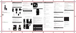
(Handset)
KX-TGA661RUB/RUM
KX-TG6611RUB/RUM
/UAB/UAM/CAB/CAM
(Base Unit)
AOH and Caller ID Compatible
(Charger Unit)
Model No
Base Unit
Handset Charger Unit Expandable
KX-TG6611 1 (TG6611) 1 (TGA661)
Up to 6
KX-TG6612 1 (TG6611) 2 (TGA661)
1
Up to 6
KX-TGA661* 1 (TGA661)
Configuration for each model
1
*KX-TGA661 is also an optional accessory, which contains a
handset and a charger.