background image


Technical Guide 


Colour Television 


GP 31 Chassis 


Circuit Explanations 


Panasonic


Panasonic AVC Networks  

Kuala Lumpur Malaysia Sdn. Bhd. 

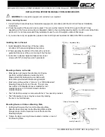
Summary of Contents for GP 31

Page 1: ...1 Technical Guide Colour Television GP 31 Chassis Circuit Explanations Panasonic Panasonic AVC Networks Kuala Lumpur Malaysia Sdn Bhd ...

Page 2: ... Audio Circuit 4 1 Audio Processor 17 4 1 1 Sound Processor 17 4 1 2 Audio Amplifier 17 5 Deflection Circuit 5 1 Horizontal Output Circuit 20 5 1 1 Horizontal Output Operation 21 5 2 Vertical Output Circuit 23 5 2 1 Vertical Output Operation 23 6 Colour Output 6 1 Colour Output Stage 24 7 Protection Circuit 25 8 Power Circuit 8 1 Start up Circuit 29 8 2 Output Voltage Control 29 8 3 Regulation 30 ...

Page 3: ...e or repair the product or products dealt with in this service information by anyone else could result in serious injury or death Introduction We at Panasonic realise that the service engineer needs to understand the circuitry inside the TV and for this need we have produced this Technical Guide This Technical Guide contains information for GP 31 chassis and should be used in conjunction with the ...

Page 4: ...4 Location of Control Circuit Boards Board Name Function A Board Main Board L Board CRT Board A Board L Board ...

Page 5: ...5 GP 31 Chassis Block Diagram ...

Page 6: ...g 1 0 2 The aerial intercepts the TV signal and amplified by the RF amplifier 3 The local oscillator generates basic frequency to convert RF signal into IF signal intermediate signal in the mixer 4 Here the IF signals is output to UOC IC601 for video and sound processing 1 2 IF Control Control of internal Tuner IF processing is performed by the UOC IC601 the IC601 sending control information via I...

Page 7: ...7 UOC IC601 ...

Page 8: ...ng Multi standard colour decoder with automatic search system Internal base band delay line Horizontal and vertical geometry processing OSD text gain reduction control White point and black level off set adjustment b Micro controller 80C51 micro controller core standard instruction set and timing 1 µs machine cycle 128K byte ROM 12K byte RAM Data Back up Storage of tuning switching control and adj...

Page 9: ...n 1 EEPROM IC1103 These memories are 1K byte non volatile memories of microchips and bit pattern of 1024 x 8 bits 2 Tuner TU001 To select a desired channel signal from the several RF signal from TV stations and convert the selected RF signal into a signal of an intermediate frequency IF 3 Sound Processor IC2101 The sound processor IC will cover the sound processing of all analog TV Standards world...

Page 10: ...AC data and each SUB DAC data CUT OFF RGB DRIVE etc 10 PICTURE MENU SOUND MENU 11 AVL Pin No Name Function 1 A0 GROUND 2 A1 GROUND 3 A2 GROUND 4 GND GROUND 5 SDA Serial Data In Out 6 SCL Serial Clock Input 7 WP Write Protect Input 8 VCC 5V 2 4 Reset circuit 1 Power on reset is generated internally to the UOC IC601 hence no external reset is required The TV processor generates the master reset in t...

Page 11: ...put 17 VDRA Vertical drive A output 18 IFIN1 IF input 1 19 IFIN2 IF input 2 20 IFREF Reference current input 21 VSC Vertical sawtooth capacitor 22 AGCOUT Tuner AGC output 23 DEFM SIF input 1 24 DECUP SIF input 2 25 GND2 Ground 2 for TV processor 26 SNDPLL Narrow band PLL filter 27 FSC Sub carrier reference output 28 AV1L Audio 1 Left input 29 AV2R Audio 2 Right input 30 HOUT Horizontal output 31 F...

Page 12: ... core 3 3V 62 OSCGND Oscillator ground supply 63 XTALIN Crystal oscillator input 64 XTALOUT Crystal oscillator output 65 RESET Not used 66 3 3V Digital supply to periphery 3 3V 67 LED Red LED Wake up timer Normal H STDBY L Power off Wake up H ON 1 sec L OFF 1 sec Protect Mode 0 5 sec ON 4 sec OFF 68 YUV L SW Input for YUV H YUV Input L Manual 69 REM IN Input for the remote control signal 70 STDBY ...

Page 13: ...13 Video Circuit ...

Page 14: ... sound trap at pin 38 to remove the unwanted SIF component and output signal is fed to pin 40 IC601 Video inputs from AV1 pin 42 AV2 pin 44 and IF signal are fed to internal Video Switch The selected video signal will go through YC separation and colour decoding where output YUV is then fed to an internal YUV switch YUV signal is input at pin 52 53 and 51 to IC601 Internal YUV switch will feed the...

Page 15: ...15 Audio Circuit Stereo AV Stereo ...

Page 16: ...16 Mono ...

Page 17: ...als from AV terminals are fed to pin 53 54 AV1 pin 56 57 AV2 and pin 47 48 YUV of MSP IC2101 for sound processing SIF signal from UOC IC601 pin 33 is fed to pin 67 of IC2101 The audio signals are then fed to Audio amplifier IC2301 before output to loudspeakers For AV STEREO model audio signals from AV terminals are fed to pin 53 54 AV1 pin 56 57 AV2 and pin 47 48 YUV of MSP IC2101 SIF signal is fr...

Page 18: ...18 Deflection Circuit ...

Page 19: ...19 Horizontal Output Circuit COLLECTOR FBT 140V H DRIVE FBI H OUT ...

Page 20: ... function of sending the deflection current to DY in order to make the electrical beam scans horizontally Beside this it also has an additional function of generating a high voltage in the second stage voltage coil of the Flyback Transformer T501 and supplying this voltage to the CRT anode pole and the focus pole 4 A number of voltages are taken for using in Focus CRT and Heaters etc from the seco...

Page 21: ...l t3 t4 5 Then the deflection coil current begins charging the capacitor with an opposite characteristic in the LC only resonance circuit 6 However since the damper diode D is connected the deflection coil voltage between terminals biases the diode in a forward direction the deflection coil current does not flow in to the resonance capacitor so the damper current flows into the diode As a result t...

Page 22: ...22 Vertical Output Circuit Vcc DY V V PROTECTION 8V ...

Page 23: ... 1 7 2 This vertical output IC IC451 consists of an operational amplifier to which the vertical pulse in the form of a sawtooth is passed pin 1 the results of which are output via pin 5 3 IC451 also contain a pump up circuit which is used to provide a switching voltage for the vertical flyback period This is required as the energy requirement of the vertical output stage is highest during flyback ...

Page 24: ...oard The RGB signals fed to the colour output stage are fed from IC601 located on the A Board from pins 56 R 57 G 58 B Here the signal is then fed to IC351 pin 1 R pin 2 G pin 3 B to the inverting input of an operation amplifier The signals are output via pin 9 R pin 8 G and pin 7 B to drive the CRT cathodes Fig 6 1 R IN G IN B IN B OUT G OUT R OUT GND 8V BLK 210V ...

Page 25: ...ion input Pin 34 of IC601 is intended for overvoltage X ray protection B 140V overcurrent protection and vertical drive protection 3 When this protection is activated the horizontal drive is directly switched off protection mode 4 Pin 34 of the UOC IC601 is pulled HIGH resulting TV being switched into standby mode protection mode after a short delay and LED starts blinking Fig 7 0 ...

Page 26: ...520 ON D520 ON Q580 ON Q581 ON D583 ON Pin 34 of UOC HIGH Protection mode LED blink Overvoltage Of CRT Heater in X Ray Protector Circuit When the heater voltage exceeds the zener D511 breakover voltage a HIGH level is applied to base of Q580 D511 ON X ray protector circuit Q580 ON Q581 ON D583 ON Pin 34 of IC601 HIGH Protection mode LED blink Excessive Voltage In Vertical Deflection Chip IC451 Whe...

Page 27: ...27 GP31 Power Map ...

Page 28: ...28 Power Circuit IC802 13V 140V AC MAIN 11V 5V RELAY ...

Page 29: ...6 however slows this decreasing voltage at pin 4 long enough to prevent the shut down voltage of 9 7V being reached thus allowing the drive winding voltage at V1 V2 to become established 6 If voltage at pin 4 falls below 9 7V IC801 stop functioning 8 2 Output Voltage Control 1 When the internal MOSFET transistor of IC801 conducts the current flows via the primary winding P1 and P2 of T801 and IC80...

Page 30: ...ieved by the use of the photocoupler IC860 2 The photocoupler current varies in response to the current drawn via pin 2 of IC802 3 IC802 is used to monitor the B supply by comparing the B secondary voltage with an internally established reference voltage within IC802 which in turn controls the current drawn via pin 2 4 If either the AC mains input voltage gets higher or the load current on the sec...

Page 31: ... begins to rise again but when it reaches the start up level 18 2V the latch circuit continues to stop the drive 3 When latch is ON Vin terminal pin 4 voltage increases and decreases within the 9 7V to 18 2V range 4 Cancellation of the latch is achieved by switching OFF the TV 8 7 Stand by Operation 1 The stand by power supply circuit keeps the IR UOC IC601 and EEPROM IC1103 operational during sta...

Reviews: