background image

©

2006 Matsushita Electric Industrial Co., Ltd. All

rights

reserved.

Unauthorized

copying

and

distribution is a violation of law.

Vol. 1

Colour

(S).......................Silver Type

DVD Recorder

ORDER NO.CHM0605031CE

Summary of Contents for DMR-EH65EE

Page 1: ... 2006 Matsushita Electric Industrial Co Ltd All rights reserved Unauthorized copying and distribution is a violation of law Vol 1 Colour S Silver Type DVD Recorder ORDER NO CHM0605031CE ...

Page 2: ...HDMI Block Diagram 50 13 Schematic Diagram 51 13 1 Interconnection Schematic Diagram 51 13 2 Power Supply Schematic Diagram 52 13 3 Main Net 1 4 Section Main P C B 1 4 Schematic Diagram M 53 13 4 Main Net 2 4 Section Main P C B 1 4 Schematic Diagram M 54 13 5 Main Net 3 4 Section Main P C B 1 4 Schematic Diagram M 55 13 6 Main Net 4 4 Section Main P C B 1 4 Schematic Diagram M 56 13 7 A V I O 1 4 ...

Page 3: ...o measure the potential across the resistor 4 Check each exposed metallic part and measure the voltage at each point 5 Reverse the AC plug in the AC outlet and repeat each of the above measurements 6 The potential at any point should not exceed 0 75 volts RMS A leakage current tester Simpson Model 229 or equivalent may be used to make the hot checks leakage current must not exceed 1 2 milliampere ...

Page 4: ...y a grounded tip soldering iron to solder or unsolder ES devices 4 Use only an anti static solder removal device Some solder removal devices not classified as anti static ESD protected can generate electrical charge sufficient to damage ES devices 5 Do not use freon propelled chemicals These can generate electrical charges sufficient to damage ES devices 6 Do not remove a replacement ES device fro...

Page 5: ...2 2 Precaution of Laser Diode 5 DMR EH65EE DMR EH65GC DMR EH65GCS DMR EH65GN ...

Page 6: ...The lead free solder has to be used when repairing the equipment for which the lead free solder is used Definition The letter of PbF is printed on the PCB using the lead free solder To put lead free solder it should be well molten and mixed with the original lead free solder Remove the remaining lead free solder on the PCB cleanly for soldering of the new IC Since the melting point of the lead fre...

Page 7: ...3 Service Navigation 3 1 Service Information 3 2 Caution for DivX 7 DMR EH65EE DMR EH65GC DMR EH65GCS DMR EH65GN ...

Page 8: ...4 Specifications 8 DMR EH65EE DMR EH65GC DMR EH65GCS DMR EH65GN ...

Page 9: ...9 DMR EH65EE DMR EH65GC DMR EH65GCS DMR EH65GN ...

Page 10: ...10 DMR EH65EE DMR EH65GC DMR EH65GCS DMR EH65GN ...

Page 11: ...r unit Visit www divx com vod for more information Display unit s registration code 5 New Feature 5 1 About DivX 5 1 1 General DivX is a new video compressing format that is applied MPEG4 technology to improve image quality and the compressibility and it is developed by the DivXNetworks Inc Video file of high resolution and the high picture quality can be made though it is a high compressibility D...

Page 12: ...12 DMR EH65EE DMR EH65GC DMR EH65GCS DMR EH65GN ...

Page 13: ...13 DMR EH65EE DMR EH65GC DMR EH65GCS DMR EH65GN ...

Page 14: ...14 DMR EH65EE DMR EH65GC DMR EH65GCS DMR EH65GN ...

Page 15: ...h registration of number of playback as Divx file Number of playback of rental file is counted by the recorder When rental file is played remaining number of times that can be played back will be shown to users recorder requests users to input yes or no Following specifications have been installed for the rental files in the purpose to clarify the count condition of number of times of playback Con...

Page 16: ...atic Input switch 2 Link of Power In case setting of FUNCTIONS Setup TV Screen Functions of HDMI Control with HDMI are on all above equipments Link functions are effective 5 2 3 Outline of Equipments Linked functions 1 Automatic Input switch At starting of playback GUI display by DIGA it turns on power of VIErA and it displays picture of DIGA onto screen of VIErA Starting of playback It includes a...

Page 17: ...splay While Timer recording is being executed Functions is being displayed are included 2 Case that DIGA is playing back only North America Japan However except cases below During EE display but manual recording is being executing during EXT_Link recording During Tray is being opened Case that DIGA is in status that power cannot turn off during dubbing during finalize 17 DMR EH65EE DMR EH65GC DMR ...

Page 18: ... Controls and Components Followings are the Location of Controls and Components for DMR EH65GC GCS GN as a sample For other model refer to each Operation Instructions 18 DMR EH65EE DMR EH65GC DMR EH65GCS DMR EH65GN ...

Page 19: ...19 DMR EH65EE DMR EH65GC DMR EH65GCS DMR EH65GN ...

Page 20: ...y on the front panel for over 10 seconds to turn off the power forcibly and press STOP CH UP keys on the front panel simultaneously for 5 seconds 7 1 2 When the Forcible Disc Eject can not be done 1 Turn off the power and pull out AC cord 2 Remove the Top Case 3 Put deck so that bottom can be seen 4 Slide SLIDE CAM by Eject Pin JZJ0484 or minus screw driver small in the direction of arrow to eject...

Page 21: ... its recovery process No display U99 Hang up Displayed when communication error has occurred between Main microprocessor and Timer microprocessor No display Displayed is left until the POWER key is pressed H19 Inoperative fan motor When inoperative fan motor is detected after powered on the power is turned off automatically The event is saved in memory No display No display F00 No error informatio...

Page 22: ... ERR is displayed when start up of HDD was failed Except error of setting of Power on Stand by a When normal start up was failed b When start up at HDD boot was failed c When start up from state of P OFF was failed d When start up from state of HDD SLEEP was failed HDD ERR is displayed when above each start up of HDD was failed In case b tray opens automatically and HDDERR is displayed until versi...

Page 23: ...ess STOP and OPEN CLOSE simultaneously for 5 seconds Forced power off When the power button is not effective while power is ON turn off the power forcibly When Timer REC is ON or EXT LINK is ON execute Forced Power off after releasing Timer REC or EXT LINK Display in P off mode Press Power key over than 10 seconds Aging Perform sequence of modes as Aging Description shown below continually Display...

Page 24: ...The progressive setting is initialized to Interlace The display before execution leaves When the power is on E E mode press STOP and PLAY simultaneously for 5 seconds 8 1 3 Service Modes at a glance Service mode setting While the power is off press REC CH UP and OPEN CLOSE simultaneously for five seconds Item FL display Key operation Mode name Description Remote controller key Release Items Item o...

Page 25: ... service mode Switch Interlace Progressive Press 1 4 in RTSC Return XP mode I P are switched alternately Audio 44 1 kHz 48 kHz Switch Press 2 4 in RTSC Return XP mode 48 kHz 44 1 kHz are switched alternately I P Switch Switch Interlace and Progressive in EE mode Initial setting is Interlace This command is effective during executing White Picture Output Magenta Picture Output and RTSC Return in XP...

Page 26: ...ode while executing do forced power off Method Press the POWER button more than 10 seconds Laser Used Time Indiction Check laser used time hours of drive l is the used time display in hour lLaser used time of DVD CD in Playback Recording mode is counted Press 4 1 in service mode Delete the Laser Used Time Laser used time stored in the memory of the unit is deleted Press 9 5 in service mode 26 DMR ...

Page 27: ...1 1 9 In case that the maker cannot be identified display is black out Delete the Last Drive Error Delete the Last Drive Error information stored on the DVD RAM Drive Press 9 6 in service mode Laser power confirmation Drive state is judged based on difference between laser power value at shipping and present laser power value If DVD RAM disc in not inserted NO DISC is displayed If power value stud...

Page 28: ...MAIN CPU 02 Defect of RAM Drive 03 Defect of Disc 04 Defect of Digital P C B or Communication Error 05 Defect of Digital P C B AV DEC MAIN CPU 06 Defect of HDD Display the time when the error has occurred for 5 seconds DD Day hh Hour mm Minute Accumulated working time till occuring of the error is left displayed Indicating unit Second Press 6 5 in service mode Then press 0 1 1 9 the past 19 error ...

Page 29: ...Press 8 4 in service mode P50 L Output Timer Microprocessor IC7501 76 output Low signal for AV1 pin 10 passing through inverter approx 4 4V DC at AV1 pin 10 When OK When NG Press 8 5 in service mode Tray OPEN CLOSE Test The RAM drive tray is opened and closed repeatedly is number of open close cycle times Press 9 1 in service mode When releasing this mode press the POWER button of Remote Controlle...

Page 30: ...40 Pin New RFKZ0168 Extension Cable Power P C B Fan Motor 3 Pin Same as E50 E55 Series RFKZ0339 Extension Cable MainP C B HDD 4 Pin New JZS0484 Eject Pin Same as E50 Series RFKZ03D01K Lead Free Solder 0 3mm 100g Reel New RFKZ06D01K Lead Free Solder 0 6mm 100g Reel New RFKZ10D01K Lead Free Solder 1 0mm 100g Reel New RFKZ0316 Solder Remover Lead free 10W temperature Solder 180g New RFKZ0328 Flux New...

Page 31: ...The following chart is the procedure for disassembling the casing and inside parts for internal inspection when carrying out the servicing To assemble the unit reverse the steps shown in the chart below 10 2 P C B Positions 31 DMR EH65EE DMR EH65GC DMR EH65GCS DMR EH65GN ...

Page 32: ...on of the arrows 10 4 Front Panel 1 Unlock 6 tabs in A F turn Pull with the front panel in the direction of your side 10 5 SD Card P C B 1 Remove 1 FFC and 2 screws A to remove SD Card P C B 10 6 RAM Digital P C B Module Note After replacing RAM Digital P C B Module TM AV1 is displayed on FL Once power off and start up again 32 DMR EH65EE DMR EH65GC DMR EH65GCS DMR EH65GN ...

Page 33: ...s to remove Digital P C B 3 Put Digital P C B on RAM Drive and remove RAM Digital P C B Module Note RAM Digital P C B Module as service part has no heat sink unit Before returning to customer heat sink unit should be installed on Digital P C B 33 DMR EH65EE DMR EH65GC DMR EH65GCS DMR EH65GN ...

Page 34: ...10 7 DV Jack P C B 1 Remove 1 Screw A to remove DV Jack P C B 10 8 HDD 34 DMR EH65EE DMR EH65GC DMR EH65GCS DMR EH65GN ...

Page 35: ...2 Remove 4 Screws A to remove HDD Angle with HDD 3 Put HDD with HDD Angle up and down inversely so as not to give a shock to HDD 4 Remove 4 screws A remove HDD 10 9 Rear Panel 1 Disconnect Fan Connector 35 DMR EH65EE DMR EH65GC DMR EH65GCS DMR EH65GN ...

Page 36: ...anel 10 9 1 Fan Motor 1 Disconnect Fan Connector and remove 2 Screws A 2 Push and unlock 2 Locking Tabs A to remove Fan Motor 10 10 Power P C B 1 Remove 1 Screw A 2 Remove 3 Screws B and disconnect Connector A to remove Power P C B 36 DMR EH65EE DMR EH65GC DMR EH65GCS DMR EH65GN ...

Page 37: ...A and 1 Screw B 3 Remove Digital Angle to remove Main P C B and Front L P C B 10 12 Tuner P C B 1 Pull out the Tuner P C B in the direction of the arrow 10 13 HDMI P C B 1 Pull out the HDMI P C B in the direction of the arrow 37 DMR EH65EE DMR EH65GC DMR EH65GCS DMR EH65GN ...

Page 38: ...rements and Adjustments 11 1 Service Positions Note For description of the disassembling procedure see the section 10 11 1 1 Checking and Repairing of Power P C B 38 DMR EH65EE DMR EH65GC DMR EH65GCS DMR EH65GN ...

Page 39: ...11 1 2 Checking and Repairing of RAM Digital P C B Module 39 DMR EH65EE DMR EH65GC DMR EH65GCS DMR EH65GN ...

Page 40: ...11 1 3 Checking and Repairing of Main P C B 40 DMR EH65EE DMR EH65GC DMR EH65GCS DMR EH65GN ...

Page 41: ...11 1 4 Checking and Repairing of HDD 41 DMR EH65EE DMR EH65GC DMR EH65GCS DMR EH65GN ...

Page 42: ...11 2 Caution for Replacing Parts 11 2 1 Items that should be done after replacing parts 42 DMR EH65EE DMR EH65GC DMR EH65GCS DMR EH65GN ...

Page 43: ... 9 Press Power button to turn off power 10 Press Power button to turn on power 11 HELLO SELF CHECK are displayed on FL 12 UNFORMAT is displayed on FL 13 After UNFORMAT was displayed message to request FORMAT is displayed on TV screen 14 Select Yes and press ENTER key to format HDD After FORMAT program in HDD will be lost but Main firm will not be lost Write of the main farm is completed above Driv...

Page 44: ...ack In case of that the trouble is caused by SD card and or DV terminal Models with SD Card or DV Input Jack 1 SD Card Check to be able to display and copy the picture 2 DV terminal Check to be able to record from DVC 8 After checking and making repairs upgrade the firmware to the latest version Make sure that FIRM_SUCCESS appears in the FL displays UNSUPPORT display means the unit is already upda...

Page 45: ...DR 12V DR P ON IC7501 42 SECTION TIMER FROM ON QR1501 E FET D S G Q1509 DR 12V OUT 1 2 3 5 6 7 8 4 AC INLET P1101 SURGE SUPPRESSOR AND SURGE ABSORBER F1101 VA1110 L1120 D1140 C1143 RECTIFIER T1150 POWER SWITCHING TRANSFORMER 12 P1 2 1 3 4 9 5 IC1150 SWITCHING IC VCC GND Z C F B 10 8 7 P2 V2 V1 7 VIN S2B S2A S1A S1B 2 3 4 5 1 3 2 D1270 2 1 IP1601 SWITCHING QR1800 QR1801 1 2 7 6 Vin PW ON FET Gate D...

Page 46: ...gram 35 Except EG 6 3 IC7301 IC7302 1 3 VDD OUT RESET 26 IC7301 FB S CS EXT D 2 6 5 1 G 3 Q59501 REG D 12V 4 8 ON OFF 2 5 7 VIN 1 IC59501 DC DC CONVERTER IC50001 IC53003 IC53202 IC53203 5V IC50001 IC53001 IC53003 IC57001 3 3V VIN 1 2 3 VOUT REG D 3 3V IC50001 IC55004 I C55006 IC57001 3 3V Q7513 IC50001 IC50002 IC50004 3 3V 12V IC59504 ON D 3 8V 60 62 P7402 P59001 ANA 3 3V D 3 3V 56 P7402 P59001 42...

Page 47: ... a b SW9 OUT V AV4 24 23 a b SW8 OUT C AV4 22 SW7 a b OUT Y AV4 20 19 OUT G AV1 17 6MHz SW5 12MHz a b c 15 OUT Y COMP 14 SW6 a b c d OUT B AV1 12 OUT B Y COMP 11 6MHz SW4 12MHz a b c d OUT R C AV1 9 SW3 a b c VIDEO PROCESSOR IC3001 OUT R Y COMP 7 SW2 a b c SW1 12MHz 6MHz CLAMP BIAS CLAMP CLAMP BIAS CLAMP LPF 6MHz CLAMP BPF 6MHz BIAS a b CLAMP BIAS c b a AV2 V Y AV2 B AV2 G AV2 R C AV3 V AV3 C AV3 ...

Page 48: ...UDIO 15 14 PS7801 PP7401 4 PS7801 PP7401 5 NICAM A2 IC7301 SIF IN MONO L OUT R OUT 1 2 25 38 TUN Lch 62 54 TUN Rch AV4 TUN SA5L BUFF e d c b a SA1L e d c b a SA3L e d c b a SA2L 58 AV3 Lch FRONT AV3 FRONT INPUT JACK JK3002 AUDIO Lch MONO LINE Rch LINE 9 10 11 12 13 d c b a SA4R SELECT SWITCH OUTPUT AV3 Rch 50 SA5R TUN AV4 BUFF e d c b a SA2R AUDIO IN ch1 L AUDIO IN ch2 R AUDIO IN ch1 L AUDIO IN ch...

Page 49: ...2 FAN LOCK H 39 TBUS CLK 35 37 P7402 SCLK P7402 SBPTM DR POWER ON 42 KEY IN1 S7504 EE OPEN CLOSE IR QR4003 XT MUTE 85 IC3001 SLICER VIDEO KEY IN3 KEY IN2 Q7501 Q7503 12 PP7401 PS7801 PS7801 PP7401 8 7 30 29 30 29 IIC DATA IIC CLK DMR EH65EE GC GCS GN Timer Block Diagram POWER SUPPLY SECTION TO TU POWER ON DI POWER ON 43 44 P OFF U V TUNER TU7801 SDA XIN XOUT 15 HDMI CEC IN 20 HDMI CEC OUT 78 13 10...

Page 50: ... P55002 FP56101 P55002 39 31 29 27 25 2 10 12 14 16 FP56101 P55002 FP56101 P55002 FP56101 P55002 FP56101 P55002 FP56101 P55002 20 19 21 22 FP56101 P55002 FP56101 P55002 FP56101 P55002 FP56101 P55002 FP56101 P55002 7 6 4 3 1 12 13 10 9 P56102 L56101 L56102 L56103 L56104 P56102 P56102 P56102 P56102 P56102 P56102 P56102 P56102 TX2P TX2M TX1P TX1M TX0P TX0M TXCP TXCM 16 15 P56102 3V 5V Conv 3V 5V Conv...

Page 51: ..._L3 YOUT_DM UARTM2P DGND UARTP2M DGND DGND DGND IECOUT DGND X_SW_3R2V D3R3V MIXROUT_DM 88 87 86 85 84 83 82 81 80 79 78 77 76 75 74 73 72 71 70 69 68 67 66 65 64 63 62 61 60 59 58 57 56 55 54 53 52 51 50 49 48 47 46 45 44 43 42 41 IT_CK MIXLOUT_DM I2C5CK AUGND I2C5DT AUGND D3R3V AUGND XFWE AADC_R P_OFF_L2 AADC_L ITA2M XDMUTE ITM2A AU5V DR5V XMPREQ DR5V DRGND SBPTM DRGND XINTM DR12V SCLK DR12V XINT...

Page 52: ... 8 1 3 4 2 23 22 K1KB23A00004 TO P1501 MAIN P C B MAIN NET 1 4 SECTION P1102 L1270 G0A100H00025 VWJ0795 5 LB1123 C1143 F2B2W4700003 D1141 B0AAGR000003 2 3 1 11 10 12 6 4 5 8 7 9 ETS28BF1W6AD T1150 ECQU2A223MLC C1121 K1123 VWJ0795 10 4 3 1 2 B0EDKT000009 D1140 3 1 2 B0JBSG000010 D1270 LB1124 VWJ0795 5 4 7 2 1 3 9 5 C0DACZH00017 IC1150 ERJ6GEY0R00V LB1126 22 F2A1V6800002 C1150 EEUFM1V680B 35V68 JG B...

Page 53: ...X_SW12V X_SW12V X_SW3R8V X_SW3R8V 21 22 20 FANLOCK FAN_GND 23 FANOUT P_SAVE_L X_SW12V P T T X_SW15R5V ANA3R3V ANA5V NC NC X_SW5R2V MM1685C NC CN GND V OUT ON H V IN NC GND V IN V OUT ON H TUREG5V PG050DNA1ZPH VO NC VIN CNT GND S 815A33AMC I2STFG X_SW3R3 NC CN GND CNT VIN GND VO NC V OUT NC NC V IN ON H MM16830 S 815A50AMC I3JTFG 1 2 3 4 5 6 7 8 9 10 P_SAVE_L T FANLOCK T FANOUT T X_SW_3R8V T 5 4 3 ...

Page 54: ... 2 4 5 IC7402 C0CBCDC00052 4 2 1 3 5 IC7401 C0CBCYG00004 AFC SIFOUT UNREG38V IICDATA AUDIOOUT GND GND GND PS5V BOOSTER5V SW2 IICCLK GND TUREG5V CPSVOUT EB DE DE T DE TUNERVIDEOIN TUNER PACK RFC_AUDIO EB RFC_AMUTE EB CN NC GND ON H VIN NC MM1685A NC VOUT T PS5V AV AV AV T T T AV T T T T AV AV UN5213 TX T T DE T AV GND VIN ON H VADJ PQ200WNA1ZPH VOUT BOOSTER 5V PS11R6V VO NC GND CNT VIN S 815A50AMC ...

Page 55: ...DGND DGND 61 DGND 57 59 BPBOUT_DM COUT_DM YOUT_DM RPROUT_DM MIXLOUT_DM MIXROUT_DM GPYOUT_DM CPNCIN_DM 75 DGND 73 DGND 69 71 V_YIN_DM 77 DGND DGND 85 G_IN 83 BS_ON 79 81 DGND A B C D E F G 1 2 3 4 5 7 6 C1527 1 R1506 2200 6 7 5 2 4 3 8 1 B1DHED00008 Q1501 C1529 10V470 C1516 50V150 6 7 5 2 4 3 8 1 B1DHED000008 Q1509 R1507 8200 QR1503 UNR521300L C1526 1 C1519 1 C1528 1 R1505 82K 25V100 C1541 2 1 4 3 ...

Page 56: ..._A AV G_R_C_IN_A AV T T T AV NC VCC NC SCL SDA VSS VE NC X_SW_12V 68 24 DR5V 16 18 DR12V DRGND 14 DR12V DR5V DRGND 22 20 12 DGND 4 6 DGND DGND 2 DGND DGND DGND 10 8 D3R3V 36 I2C5DT 34 DGND IT_CK IECOUT I2C5CK X_SW3R8V X_SW_12V X_SW_12V X_SW3R8V 64 66 62 UARTM2P 52 50 P_OFF_L3 40 44 42 38 UARTP2M 48 46 X_SW3R2V D3R3V ANA3R3V 58 60 EPG_ON_H BUSY 54 56 CSYNC_IN ITM2A 26 XFWE ITA2M 30 32 P_OFF_L 28 76...

Page 57: ... IC DETAIL BLOCK DIAGRAM IC7401 PS 11 6V SWITCHING REGULATOR IC DETAIL BLOCK DIAGRAM IC7403 PS 5V SWITCHING REGULATOR IC DETAIL BLOCK DIAGRAM IC1505 XSW 3 3V SWITCHING REGULATOR IC DETAIL BLOCK DIAGRAM IC1521 ANA 3 3V SWITCHING REGULATOR IC DETAIL BLOCK DIAGRAM IC7402 BOOSTER 5V SWITCHING REGULATOR IC DETAIL BLOCK DIAGRAM IC1520 ANA 5V SWITCHING REGULATOR IC DETAIL BLOCK DIAGRAM IC1522 RESET IC DE...

Page 58: ...G R4076 820 16V22 C4063 R4093 120 ECJ1VF1C104Z C4065 C4061 ECJ1VF1C104Z R4081 820 R4001 ERJ3GEY0R00V 33P 22 C4057 G_MIXROUT_A R4057 D0HB123ZA002 16V22 C4034 D0HB682ZA002 R4047 R4089 2700 2SD132800L Q4009 C4083 ECJ2VC1H561J 3 1 2 D4006 MA3Z142D0LG MA142WA TX 2SD1328 TX IN1 VEE MA142WA TX IN2 2SD1328 TX 2SD1328 TX 2SD1328 TX VO1 IN1 GND VOUT NR ON H VIN IN2 VCC VO2 VEE IN2 IN1 M VCC VO2 IN2 VO1 UN52...

Page 59: ...20 T S AV3 IN C DECODER Y M 4 8 7 9 5 6 13 10 12 11 15 14 9 5 2 1 4 3 7 8 6 16 15 17 11 12 AV1 10 14 13 2 3 1 AV2 18 20 21 19 17 16 MA165TA5VT TV GND VIDEO OUT VIDEO IN Y IN GND V IN BLUE GREEN DATA AV2 12V CONTROL GND BLUE RED C IN GND RED BLUE GND A PB 12V GND GREEN GND A DATA GND RED CONTROL RED C OUT GND BLUE VIDEO IN BLANKING GND V IN GND V OUT GND BLANK GND GREEN AUDIO IN CH2 R AUDIO OUT CH2...

Page 60: ...5 6 7 8 9 10 11 12 13 14 15 16 17 18 20 19 21 22 5 4 3 2 1 C B A B TO A V I O SECTION 1 4 NOTE DO NOT USE THE PART NUMBER SHOWN ON THIS DRAWING FOR ORDERRING THE CORRECT PART NUMBER IS SHOWN IN THE PARTS LIST AND MAY BE SLIGHTLYDIFFERNT OR AMENDED SINCE THIS DRAWING WAS PREPARED DMR EH65EE GC GCS GN A V I O 3 4 Section Main P C B 2 4 Schematic Diagram AV M Main Net Section Page A AV A V I O Sectio...

Page 61: ...000020 0 1 C3038 SW C IN CB Y CR VCC or GND G OR M T M M M Y AV4 RCA JACK Y C NC NC AV1 LOUT AV2 ROUT AGND R AV1 ROUT AV2 LOUT NC NC 9VL 9VR DT LIN DA LIN AV2 LIN 1 2REF DA RIN TU RIN DT RIN AV1 LIN AV4 LIN 51 AV4 RIN 53 AV2 RIN 52 AV1 RIN 50 FRONT RIN 33 AV1 V IN FRONT LIN AV4 C IN AV3 C IN VCC 5V EXT CTL4 AV3 Y IN 1 2REF GND VCC 11R6V AV4 Y IN VCC ALL 5V DT C IN DT Y IN TU LIN 9VREG GND B Y OUT ...

Page 62: ... R C AV3 V AV3 C AV3 Y AV1 V 31 5 3 1 37 45 41 33 99 97 95 93 91 SA4L SELECT SWITCH OUTPUT 71 AV1 Lch 78 ADC Lch 73 AV2 Lch 74 AV2 Rch 79 ADC Rch AV1 Rch 72 LPF BUFF MUTE AGC AMP ADC Lch LPF BUFF MUTE LPF BUFF MUTE d c b a MUTE BUFF LPF AMP ADC Rch AGC MIX VCA MUTE RF OUT 76 TUN Lch 62 54 TUN Rch AV4 TUN SA5L BUFF e d c b a SA1L e d c b a SA3L e d c b a SA2L 58 AV3 Lch d c b a SA4R SELECT SWITCH O...

Page 63: ...C VSSA3 VCC VDDD1 CDE2 PCLK N C VDEC2 AF1I VSSD2 AGND NICAM AF1D TPB N C 1REF LF2 VDDR2 N C TEST2 N C VSSA2 N C ADDR1 AFR XTAL0 LF1 XTAL1 XTAL SDA OUT L VREF2 VREF P1 MONO IN EXTM VSSD3 N C EXTIL EXTL EXT IR EXTR OUTM P2 VSSA4 N C SCK AF21 SYS CLK CTRIG VDDD3 CID OUT R WS AF20 M T T IN OUT G M AV AV GND IN OUT 3 2 1 Vref PLL SC2 NARROW BAND FM DEMODULATOR PLL SC1 NARROW BAND FM DEMODULATOR 2 AMPLI...

Page 64: ...9 100 R7601 1K R7655 100 R7572 100 R7607 100 C7557 0 01 C7556 0 01 C7558 0 01 S13 S14 DP7501 A2BD00000145 R7558 2K C7542 0 1 AV AV M M GND OUT 2SD1819 TX M AV 2SD1819 TX VCC FL14 FL15 P3 1G 37 35 1GA P5 FL13 P4 P4 36 31 FL11 R8A66021GP FL21 40 P2 P2 FL20 FL24 F NX F 42 1GA 1G 45 44 NP P1 P1 41 FL23 FL26 FL25 FL17 FL18 NC P3 38 FL16 20 FL22 FL19 1GA 1G 39 CS FL00 11 FL30 12 FL29 FL28 VCC XIN RESET ...

Page 65: ...000153 C7577 0 1 X_SW_5R2V GND UNREG_38V DDGND R7616 47K LB7519 VWJ0795 5 R7615 47K MAZ4180NHF D7508 ERDS2TJ271T R7617 M M M M BD485G 5VDET or G R3111N451A TL or VDD GND OUT NC 1 2 3 4 5 6 7 8 9 10 GND VDD OUT 1 3 2 Vref F2A1C121A453 C7593 K7504 0 NOTE DO NOT USE THE PART NUMBER SHOWN ON THIS DRAWING FOR ORDERRING THE CORRECT PART NUMBER IS SHOWN IN THE PARTS LIST AND MAY BE SLIGHTLYDIFFERNT OR AM...

Page 66: ...HDMI_5VREG RFC_A_MUTE FL_100MM_H 53 NC GND TEST2 H 31 ONBOARD EPG_TXD TBUS_RXD EPG_TRIG TBUS_CLK IIC_CLK NC OPEN IIC_DATA TBUS_TXD FAN_LOCK1 HDMI_3VREG NC 5V SYNC_DET FL_CS L WIDE_H AV2_PB_L P_SAVE L DR_P_ON H DI_P_ON H AV4_SIN L TU_P_ON H HDD_PFAIL L VSYNC FL_TXD FL_RXD M1 GND SYNCIN AV NC GND AVCC 5V VDD2 5V 3R3V_OFF_H LP3 TEST1 VSS2 GND DC_R_CH AFC KEYIN1 AV2_PIN8 DC_L_CH CVIN KEYIN3 KEYIN2 79 ...

Page 67: ... 10K R7624 C7587 1 R7627 30K R7626 820 B1ABMD000004 Q7511 R7575 100 FANLOCK X_SW_12R4V 22K R7574 0 01 C7588 6 7 5 2 4 3 8 1 C0ABBA000073 IC7507 0 1 C7590 M M M B OUT V B IN B IN A IN A OUT GND A IN S7505 EVQ11A04M SELECT 8 7 6 5 1 2 3 4 B IN B IN BOUT V GND A IN A IN AOUT 10 9 8 7 6 D TO TIMER SECTION 2 4 NOTE DO NOT USE THE PART NUMBER SHOWN ON THIS DRAWING FOR ORDERRING THE CORRECT PART NUMBER I...

Page 68: ...91 96 95 99 111 110 114 116 115 112 113 107 108 103 104 100 102 101 106 105 109 121 118 119 117 120 123 1 164 42 10 8 7 9 20 17 16 19 18 22 21 12 13 11 15 14 5 4 6 38 39 34 35 30 31 25 27 26 23 24 29 28 33 32 37 36 41 40 2 3 IC56103 MN864701 HDMI_1_IRQ R656_5 1 2 82 R56156 R656_4 1 2 82 R56157 G_R656_CK_C 1 2 82 R56139 R656_6 1 2 82 R56155 R656_0 R656_1 1 2 82 R56151 R656_3 1 2 82 R56154 R656_2 1 ...

Page 69: ... TXCM SCL SDA CN GND VOUT CONT VIN SHUTDOWN THERMAL LIMITTER CURRENT DRIVER BIAS REFERENCE 8 1 2 3 4 5 6 7 H VIN VOUT NR GND ON 4 2 3 1 5 IC IC56104 3 3V SWITCHING REG IC DETAIL BLOCK DIAGRAM IC56103 HDMI TRANSMITTER IC DETAIL BLOCK DIAGRAM IC56105 5V SWITCHING REG IC DETAIL BLOCK DIAGRAM IC56107 INVERTER IC DETAIL BLOCK DIAGRAM IC56103 Detail Block Diagram IC56104 Detail Block Diagram IC56105 Det...

Page 70: ...7809 C7817 F2A0J470A599 R7811 ERDS2TJ102T 680 R7844 680 R7812 Q7802 2SB1218A0L R7816 470 C7819 33P or MSDA SDA MSCL RFAGC SCL 5V VIF SIF OUT AFT OUT BTL 30VIN AUDIO OUT VIDEO OUT VIDEOIN 5V RFC 5V TUNER SW VIF BOOSTER B AUDIO IN AFC GND IIC_DATA SIF_OUT UNREG_38V TO MAIN TUNER_VIDEO1 AUDIO_OUT GND RFC_A_MUTE GND BOOSTER_5V RFC_AUDIO SW2 IIC_CLK GND PS_5V CPS_V_OUT JC_REG_5V DMR EH65EE GC GCS GN Tu...

Page 71: ...220JV RX6801 R6804 22K SDAT2 C6801 0 01 SCMD G_SCLK_B SDAT0 SDAT1 22 R6802 SWP SDAT3 SDAT3 SDAT0 SCMD SDAT2 R6801 100 LB6801 J0JHC0000032 SDAT1 G_SCLK_B DAT3 CLK WP GND COM 3R3V CMD GND DAT1 DAT0 FG SCDA4A0200 DAT2 CD FG GND GND XSORX TPB TPA TPA TPB XDIAG XSOTX D3R3V WP CMD CD GND CLK DAT3 DAT2 DAT0 DAT1 D3R3V DMR EH65EE GC GCS GN SD Card Schematic Diagram 10 9 8 7 6 5 4 3 2 1 F E D C B A SLIGHTL...

Page 72: ...ED SINCE THIS DRAWING WAS PREPARED 13 20 DV Jack Schematic Diagram 2 1 4 3 P37002 K2HZ104B0012 2 4 3 1 6 5 K1KA06B00181 P37001 TO PS57001 DIGITAL P C B BE 2 4 SECTION TO DV JACK TPB TPA TPA IMSA 9390S 04Z901 TPB TPB TPB TPA NC NC TPA IMSA 9850B 06Z900 B 4 3 2 1 A DMR EH65EE GC GCS GN DV Jack Schematic Diagram NOTE DO NOT USE THE PART NUMBER SHOWN ON THIS DRAWING FOR ORDERRING THE CORRECT PART NUMB...

Page 73: ...2 D 3 Q1700 C 2 C1120 C 7 C1604 B 3 R1155 D 6 R1703 D 2 IP1601 B 3 C1121 B 8 C1605 B 3 R1156 D 6 R1704 D 2 QR1800 A 4 C1122 B 9 C1606 A 3 R1157 D 6 R1705 D 2 QR1801 B 4 T1150 C 5 C1123 B 9 C1607 B 2 R1158 C 6 R1800 B 4 C1125 B 5 C1608 B 2 R1200 D 3 R1801 A 4 P1101 D 8 L1120 C 8 C1143 B 6 C1701 C 3 R1201 D 3 R1802 B 4 P1102 B 1 L1270 B 2 C1150 D 6 C1702 C 3 R1205 D 4 R1803 B 4 P1103 C 1 L1400 C 3 C...

Page 74: ...2 1 Main P C B 1 4 Section 1 2 3 4 A B C EE Location Map REAR DMR EH65EE GC GCS GN Main P C B RFKB79119MT EH65EE RFKB79119NT EH65GC GCS GN 1 4 Section 1 4 2 4 3 4 4 4 FRONT DMR EH65EE DMR EH65GC DMR EH65GCS DMR EH65GN 74 ...

Page 75: ... Main P C B 2 4 Section 5 6 7 8 Location Map REAR DMR EH65EE GC GCS GN Main P C B RFKB79119MT EH65EE RFKB79119NT EH65GC GCS GN 2 4 Section 1 4 2 4 3 4 4 4 FRONT DMR EH65EE DMR EH65GC DMR EH65GCS DMR EH65GN 75 ...

Page 76: ... P C B 3 4 Section D E F Main P C B Location Map REAR DMR EH65EE GC GCS GN Main P C B RFKB79119MT EH65EE RFKB79119NT EH65GC GCS GN 3 4 Section 1 4 2 4 3 4 4 4 FRONT DMR EH65EE DMR EH65GC DMR EH65GCS DMR EH65GN 76 ...

Page 77: ... 2 4 Main P C B 4 4 Section Location Map REAR DMR EH65EE GC GCS GN Main P C B RFKB79119MT EH65EE RFKB79119NT EH65GC GCS GN 4 4 Section 1 4 2 4 3 4 4 4 FRONT DMR EH65EE DMR EH65GC DMR EH65GCS DMR EH65GN 77 ...

Page 78: ...3 D 7 C4055 D 4 C7510 D 2 R3055 B 8 R4081 C 8 R7535 E 3 R7653 E 4 Q7401 F 8 D4006 B 7 LB7411 C 4 C3014 D 7 C4056 D 4 C7511 D 2 R3056 B 8 R4088 B 7 R7536 D 3 R7655 E 4 Q7402 F 7 D7403 F 8 LB7412 B 4 C3015 E 7 C4057 C 7 C7512 D 2 R3057 B 8 R4089 B 7 R7537 D 3 Switch Q7501 D 3 D7501 F 3 LB7413 C 3 C3016 E 7 C4059 D 4 C7513 D 2 R3058 B 8 R4090 C 8 R7539 D 3 S7501 C 2 Q7502 D 3 D7502 E 4 LB7414 C 3 C30...

Page 79: ... HDMI P C B 1 A B C D 2 3 4 5 6 7 8 9 HDMI P C B Foil Side DMR EH65EE GC GCS GN HDMI P C B VEP73137A Component Side DMR EH65EE GC GCS GN HDMI P C B VEP73137A DMR EH65EE DMR EH65GC DMR EH65GCS DMR EH65GN 79 ...

Page 80: ...B and DV Jack P C B 1 A B C D 2 3 4 5 1 A B C D 2 3 4 5 DMR EH65EE GC GCS GN DV Jack P C B VEP73135A DMR EH65EE GC GCS GN Tuner P C B VEP07A91D DV Jack P C B Tuner P C B DMR EH65EE DMR EH65GC DMR EH65GCS DMR EH65GN 80 ...

Page 81: ... and Front L P C B 1 A B C D 2 3 4 5 1 A B C D 2 3 4 5 DMR EH65EE GC GCS GN Front L P C B VEP70161A DMR EH65EE GC GCS GN SD Card P C B VEP73136A Front L P C B SD Card P C B DMR EH65EE DMR EH65GC DMR EH65GCS DMR EH65GN 81 ...

Page 82: ...DMR EH65EE DMR EH65GC DMR EH65GCS DMR EH65GN 82 ...

Page 83: ...1 0 4 8 5 1 Ref No MODE 1 2 3 4 5 6 7 8 1 2 3 4 5 REC 3 3 2 0 0 4 8 4 1 0 0 5 0 5 1 PLAY 3 3 2 0 0 4 8 4 1 0 0 5 0 5 1 STOP 3 3 2 0 0 4 8 4 1 0 0 5 0 5 1 Ref No MODE 1 2 3 4 5 6 7 8 9 10 11 12 13 14 15 16 17 18 19 20 REC 2 0 2 5 1 6 0 1 6 5 0 1 6 5 0 0 4 0 3 1 6 0 4 1 7 1 7 1 6 0 4 0 1 7 1 7 PLAY 2 0 2 5 1 6 0 1 6 5 0 1 6 5 0 0 4 0 3 1 6 0 4 1 7 1 7 1 6 0 4 0 1 7 1 7 STOP 2 0 2 5 1 6 0 1 6 5 0 1 6...

Page 84: ... 0 4 9 PLAY 3 1 3 2 0 4 8 4 6 3 3 3 3 0 4 8 3 3 3 2 3 3 0 4 9 STOP 3 1 3 2 0 4 8 4 6 3 3 3 3 0 4 8 3 3 3 2 3 3 0 4 9 Ref No MODE 41 42 43 44 45 46 47 48 49 50 51 52 53 54 55 56 57 58 59 60 REC 0 4 9 4 9 4 8 0 4 9 5 0 5 0 4 9 0 4 9 0 4 8 0 0 0 0 5 0 PLAY 0 4 9 4 9 4 8 0 4 9 5 0 5 0 4 9 0 4 9 0 4 8 0 0 0 0 5 0 STOP 4 9 4 9 4 9 4 8 0 4 9 5 0 5 0 4 9 0 4 9 0 4 8 0 0 0 0 5 0 Ref No MODE 61 62 63 64 65 ...

Page 85: ...0 0 5 0 0 0 0 4 6 0 4 6 0 4 9 3 3 3 3 PLAY 18 1 5 0 18 0 0 5 0 0 0 0 4 6 0 4 6 0 4 9 3 3 3 3 STOP 18 1 5 0 18 0 0 5 0 0 0 0 5 1 0 5 1 0 1 4 9 3 3 3 3 Ref No MODE E C B E C B REC 0 9 2 0 2 5 1 12 3 5 5 PLAY 0 9 2 0 1 5 1 12 3 5 5 STOP 0 9 2 0 2 5 1 12 3 5 5 Ref No MODE E C B E C B E C B E C B E C B REC 0 0 4 9 0 0 4 9 5 1 0 1 5 1 0 0 2 3 0 5 1 0 PLAY 0 0 4 9 0 0 4 9 5 1 0 1 5 1 0 0 2 3 0 5 1 0 STOP...

Page 86: ... 0 0 3 3 0 0 0 3 3 0 Ref No MODE 81 82 83 84 85 86 87 88 89 90 91 92 93 94 95 96 97 98 99 100 REC 0 0 0 3 3 0 1 5 3 3 0 PLAY 0 0 0 3 3 0 1 5 3 3 0 STOP 0 0 0 3 3 0 1 5 3 3 0 Ref No MODE 101 102 103 104 105 106 107 108 109 110 111 112 113 114 115 116 117 118 119 120 REC 0 3 3 1 5 0 PLAY 0 3 3 1 5 0 STOP 0 3 3 1 5 0 Ref No MODE 121 122 123 124 125 126 127 128 129 130 131 132 133 134 135 136 137 138 ...

Page 87: ... 3 3 0 3 3 2 5 Ref No MODE 41 42 43 44 45 46 47 48 49 50 51 52 53 54 55 56 57 58 59 60 REC 2 5 3 2 0 1 7 0 0 0 3 3 0 3 3 1 1 0 0 3 1 5 3 3 0 1 0 4 8 PLAY 2 5 3 2 0 1 7 0 0 0 3 3 0 3 3 1 1 0 0 3 1 5 3 3 0 1 0 4 8 STOP 2 5 3 2 0 1 7 0 0 0 3 3 0 3 3 1 1 0 0 3 1 5 3 3 0 1 0 4 8 Ref No MODE 61 62 63 64 65 66 67 68 69 70 71 72 73 74 75 76 77 78 79 80 REC 0 4 8 1 1 12 3 0 12 3 1 0 12 3 0 12 3 1 3 12 3 0 ...

Page 88: ...v P7402 71 REC PLAY 1 0Vp p 20 sec div P7402 67 REC PLAY 0 6Vp p 20 sec div P7402 63 REC PLAY 1 0Vp p 20 sec div P7402 59 REC PLAY 0 6Vp p 20 sec div P7402 55 REC PLAY 0 8Vp p 20 sec div P7402 29 31 REC PLAY 0 8Vp p 1m sec div T1150 8 STOP 30Vp p 5 sec div T1150 12 STOP 10Vp p 2m sec div IC1150 1 STOP 10 0Vp p 5 sec div IC1150 9 STOP 580Vp p 5 sec div 88 DMR EH65EE DMR EH65GC DMR EH65GCS DMR EH65G...

Page 89: ...ST ADDRESS HOST DATA HOST INTERRUPT HOST READ WRITE INITIAL LOGO ABBREVIATIONS I IECOUT IPFRAG IREF ISEL IEC958 FORMAT DATA OUTPUT INTERPOLATION FLAG I CURRENT REFERENCE INTERFACE MODE SELECT L LDON LPC LRCK LASER DIODE CONTROL LASER POWER CONTROL L CH R CH DISTINCTION CLOCK M MA0 UP MCK MCKI MCLK MDATA MDQ0 UP MDQM MLD MPEG MEMORY ADDRESS MEMORY CLOCK MEMORY CLOCK INPUT MEMORY SERIAL COMMAND CLOC...

Page 90: ...E REFERENCE SOURCE POWER SUPPLY VOLTAGE W WAIT WDCK WEH WSR BUS CYCLE WAIT WORD CLOCK WRITE ENABLE HIGH WORD SELECT RECEIVER X X XALE XAREQ XCDROM XCS XCSYNC XDS XHSYNCO XHINT XI XINT XMW XO XRE XSRMCE XSRMOE XSRMWE XVCS XVDS XVSYNCO X TAL X ADDRESS LATCH ENABLE X AUDIO DATA REQUEST X CD ROM CHIP SELECT X CHIP SELECT X COMPOSITE SYNC X DATA STROBE X HORIZONTAL SYNC OUTPUT XH INTERRUPT REQUEST X TA...

Page 91: ...16 Parts and Exploded Views 16 1 Exploded Views 16 1 1 Casing Parts Mechanism Section 91 DMR EH65EE DMR EH65GC DMR EH65GCS DMR EH65GN ...

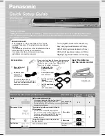
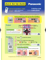
Page 92: ...16 1 2 Packing Accessories Section 92 DMR EH65EE DMR EH65GC DMR EH65GCS DMR EH65GN ...

Page 93: ...0V 0 01U 1 C3003 ECJ1VB1C104K 16V 0 1U 1 Ref No Part No Part Name Description Pcs Remarks C3004 ECJ1VB1C104K 16V 0 1U 1 C3005 ECA0JM471B 6 3V 470U 1 C3006 ECA0JM471B 6 3V 470U 1 C3007 F2A1A4710038 10V 470U 1 C3008 F2A1A1010072 10V 100U 1 C3009 F2A1A4710038 10V 470U 1 C3010 F2A1A1010072 10V 100U 1 C3011 ECJ1VB1C104K 16V 0 1U 1 C3012 F2A1A4710038 10V 470U 1 C3013 F2A1A1010072 10V 100U 1 C3014 ECJ1VB...

Page 94: ...7513 F2A1V390A386 35V 39U 1 C7514 ECJ1VB1H103K 50V 0 01U 1 C7516 ECJ1VC1H180J 50V 18P 1 C7517 ECJ1VC1H180J 50V 18P 1 C7518 F1H1H220A799 50V 22P 1 C7519 ECJ1VC1H180J 50V 18P 1 Ref No Part No Part Name Description Pcs Remarks C7520 ECJ1VB1C104K 16V 0 1U 1 C7522 ECJ1VC1H101J 50V 100P 1 C7523 ECJ1VB1H103K 50V 0 01U 1 C7524 ECJ1VB1C104K 16V 0 1U 1 C7528 ECJ1VB1C104K 16V 0 1U 1 C7531 ECJ1VC1H100D 50V 10...

Page 95: ...ion Pcs Remarks LB7415 J0JCC0000103 COIL 1 LB7416 J0JCC0000164 COIL 1 LB7417 J0JCC0000103 COIL 1 LB7418 J0JCC0000103 COIL 1 LB7419 J0JCC0000103 COIL 1 LB7420 J0JCC0000164 COIL 1 LB7501 ERJ3GEY0R00V 1 10W 0 1 LB7502 ERJ3GEY0R00V 1 10W 0 1 LB7507 ERJ3GEY0R00V 1 10W 0 1 LB7508 ERJ3GEY0R00V 1 10W 0 1 LB7509 J0JCC0000060 COIL 1 LB7510 ERJ3GEY0R00V 1 10W 0 1 LB7515 ERJ3GEY0R00V 1 10W 0 1 LB7516 ERJ3GEY0...

Page 96: ...10W 0 1 R7312 ERJ3GEYF221V 1 10W 220 1 R7313 ERJ3GEYF221V 1 10W 220 1 Ref No Part No Part Name Description Pcs Remarks R7317 ERJ3GEY0R00V 1 10W 0 1 R7319 ERJ3GEY0R00V 1 10W 0 1 R7322 ERJ3GEY0R00V 1 10W 0 1 R7324 ERJ3GEYJ221V 1 10W 220 1 R7325 ERJ3GEYJ221V 1 10W 220 1 R7326 ERJ3GEY0R00V 1 10W 0 1 R7401 ERJ3GEYJ104V 1 10W 100K 1 R7402 ERJ3GEYJ103V 1 10W 10K 1 R7403 ERJ3GEYJ153V 1 10W 15K 1 R7404 ERJ...

Page 97: ...J3GEY0R00V 1 10W 0 1 W508 ERJ3GEY0R00V 1 10W 0 1 W509 ERJ3GEY0R00V 1 10W 0 1 W510 ERJ3GEY0R00V 1 10W 0 1 W511 ERJ3GEY0R00V 1 10W 0 1 W512 ERJ3GEY0R00V 1 10W 0 1 W513 ERJ3GEY0R00V 1 10W 0 1 W514 ERJ3GEY0R00V 1 10W 0 1 W515 ERJ3GEY0R00V 1 10W 0 1 Ref No Part No Part Name Description Pcs Remarks W516 ERJ3GEY0R00V 1 10W 0 1 W517 ERJ3GEY0R00V 1 10W 0 1 W518 ERJ3GEY0R00V 1 10W 0 1 W519 ERJ3GEY0R00V 1 10...

Page 98: ...1H181J 50V 180P 1 C1606 ECJGVB1H103K 50V 0 01U 1 C1607 F2A1A6810022 10V 680P 1 C1608 ECJ2VB1E104K 25V 0 1U 1 C1701 F2A1E2210050 25V 220U 1 Ref No Part No Part Name Description Pcs Remarks C1702 ECJ1VB1C104K 16V 0 1U 1 C1703 ECJ1VB1C104K 16V 0 1U 1 C1704 ECJ1VB1C104K 16V 0 1U 1 C1705 ECJ1VC1H181J 50V 180P 1 C1706 ECJ1VB1H103K 50V 0 01U 1 C1707 F2A0J6810007 6 3V 680P 1 C1800 F2A1E4700048 25V 47U 1 D...

Page 99: ... 3V 1U 1 C56131 F1J0J106A014 6 3V 10U 1 C56132 ECJ0EB1C103K 16V 0 01U 1 C56133 F1H1A105A028 10V 1U 1 Ref No Part No Part Name Description Pcs Remarks C56134 F1H1A105A028 10V 1U 1 C56135 ECJ0EB1A104K 10V 0 1U 1 C56140 ECJ0EB1A104K 10V 0 1U 1 D56101 MA2J72800L DIODE 1 FL56101 F1H0J1050025 FILTER 1 FL56102 F1H0J1050025 FILTER 1 FL56103 F1H0J1050025 FILTER 1 FL56104 F1H0J1050025 FILTER 1 FL56105 F1H0J...

Page 100: ...06B00181 CONNECTOR 6P 1 P37002 K2HZ104B0012 CONNECTOR 104P 1 n n n n CASING ACCESSORY P ACKING 1 VEP70161A FRONT L P C B 1 RTL 2 VEP73135A DV JACK P C B 1 RTL 3 RFKB79119MT MAIN P C B 1 EE 3 RFKB79119NT MAIN P C B 1 GC GCS GN Ref No Part No Part Name Description Pcs Remarks 5 RGR0365C D1 REAR PANEL 1 EE 5 RGR0365C G1 REAR PANEL 1 GC 5 RGR0365C F1 REAR PANEL 1 GCS 5 RGR0365C E1 REAR PANEL 1 GN 6 RH...

Page 101: ...GCS A10 RQT8382 A OPERATING INSTRUCTIONS 1 IC GC A10 RQT8459 R OPERATING INSTRUCTIONS 1 ID EE A10 RQT8460 Z OPERATING INSTRUCTIONS 1 IE EE A11 RQCC2704 DVD MEDIA SHEET 1 EE A11 RQCC2705 DVD MEDIA SHEET 1 GC GCS GN PC1 RPG7869 PACKING CASE 1 EE PC1 RPG7872 PACKING CASE 1 GC PC1 RPG7871 PACKING CASE 1 GCS PC1 RPG7870 PACKING CASE 1 GN PC2 RPN1859A 2 CUSHION A 1 PC3 RPN1859B 2 CHSHION B 1 PC4 RPFC002...

Reviews: