background image

©

 Semiconductor Components Industries, LLC, 2011

March, 2017 

 Rev. 14

1

Publication Order Number:

AR0331/D

AR0331

AR0331 1/3‐Inch 3.1 Mp/Full

HD Digital Image Sensor

General Description

The ON Semiconductor AR0331 is a 1/3-inch CMOS digital image

sensor with an active-pixel array of 2048 (H) x 1536 (V). It captures
images in either linear or high dynamic range modes, with a
rolling-shutter readout. It includes sophisticated camera functions
such as in-pixel binning, windowing and both video and single frame
modes. It is designed for both low light and high dynamic range scene
performance. It is programmable through a simple two-wire serial
interface. The AR0331 produces extraordinarily clear, sharp digital
pictures, and its ability to capture both continuous video and single
frames makes it the perfect choice for a wide range of applications,
including surveillance and HD video.

The ON Semiconductor AR0331 can be operated in its default mode

or programmed for frame size, exposure, gain, and other parameters.
The default mode output is a 1080p-resolution image at 60 frames per
second (fps). In linear mode, it outputs 12-bit or 10-bit A-Law
compressed raw data, using either the parallel or serial (HiSPi) output
ports. In high dynamic range mode, it outputs 12-bit compressed data
using parallel output. In HiSPi mode, 12- or 14-bit compressed, or
16-bit linearized data may be output. The device may be operated in
video (master) mode or in single frame trigger mode.

FRAME_VALID and LINE_VALID signals are output on dedicated

pins, along with a synchronized pixel clock in parallel mode.

The AR0331 includes additional features to allow application-

specific tuning: windowing and offset, auto black level correction, and
on-board temperature sensor. Optional register information and
histogram statistic information can be embedded in the first and last 2
lines of the image frame.

The sensor is designed to operate in a wide temperature range

(–30

°

C to +85

°

C).

Features

Superior Low-light Performance

Latest 2.2 

μ

m Pixel with ON Semiconductor A-Pix

 Technology

Full HD Support at 1080 P 60 fps for Superior Video Performance

Linear or High Dynamic Range Capture

3.1 M (4:3) and 1080 P Full HD (16:9) Images

Optional Adaptive Local Tone Mapping (ALTM)

Interleaved T1/T2 Output

Support for External Mechanical Shutter

Support for External LED or Xenon Flash

Slow-motion Video (VGA 120 fps)

On-chip Phase-locked Loop (PLL) Oscillator

Integrated Position-based Color and Lens Shading Correction

Slave Mode for Precise Frame-rate Control

Stereo/3D Camera Support

Statistics Engine

www.onsemi.com

See detailed ordering and shipping information on page 2 of
this data sheet.

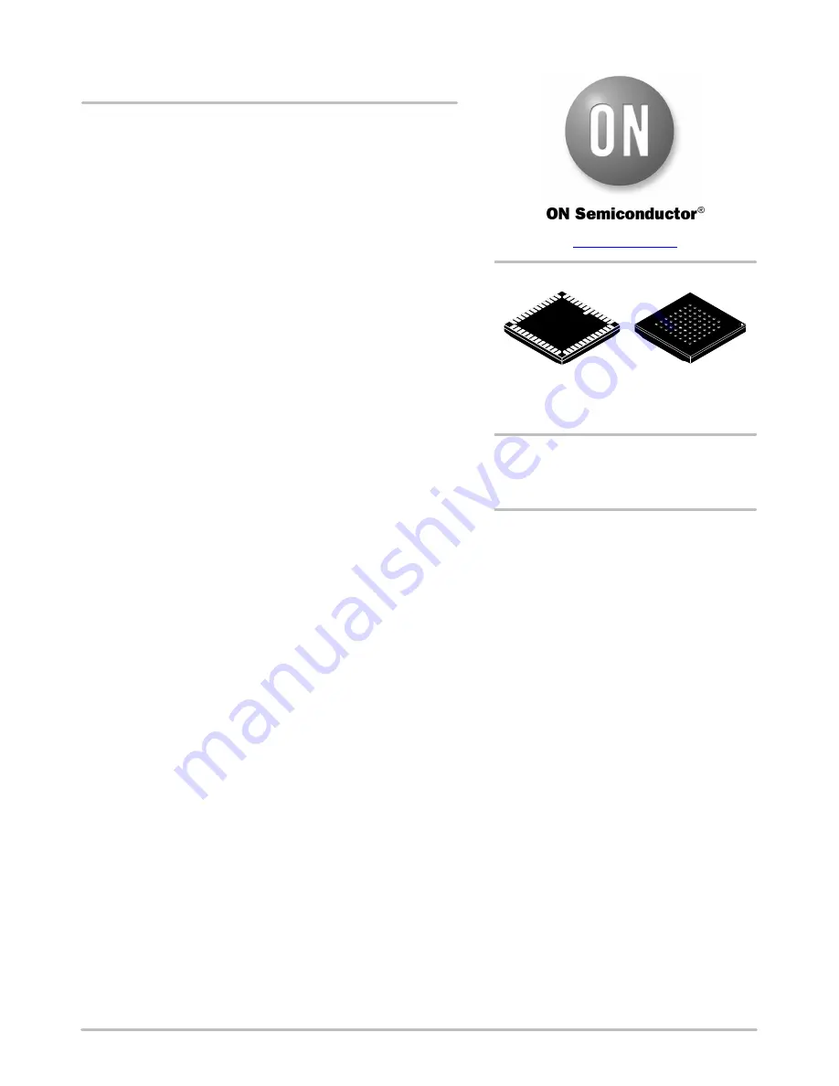
ORDERING INFORMATION

ILCC48 10x10

CASE 847AG

Data Interfaces: Four-lane Serial High-speed

Pixel Interface (HiSPi) Differential
Signaling (SLVS and HiV

CM

), or Parallel

Auto Black Level Calibration

High-speed Context Switching

Temperature Sensor

Applications

Video Surveillance

Stereo Vision

Smart Vision

Automation

Machine Vision

1080p60 Video Applications

High Dynamic Range Imaging

IBGA52 9x9

CASE 503AA

Summary of Contents for AR0331 Series

Page 1: ...e or in single frame trigger mode FRAME_VALID and LINE_VALID signals are output on dedicated pins along with a synchronized pixel clock in parallel mode The AR0331 includes additional features to allow application specific tuning windowing and offset auto black level correction and on board temperature sensor Optional register information and histogram statistic information can be embedded in the ...

Page 2: ... 48 pin iLCC HiSPi 0 CRA Dry Pack without Protective Film Double Side BBAR Glass AR0331SRSC00SHCAD3 GEVK 48 pin iLCC HiSPi 0 CRA Demo Kit 3 AR0331SRSC00SHCAD GEVK 48 pin iLCC HiSPi 0 CRA Demo Kit AR0331SRSC00SHCAH GEVB 48 pin iLCC HiSPi 0 CRA Demo Board AR0331SRSC00SUCA0 DPBR 48 pin iLCC Parallel 0 CRA Dry Pack with Protective Film Double Side BBAR Glass AR0331SRSC00SUCA0 DRBR 48 pin iLCC Parallel...

Page 3: ...l chain and digital signal chain The core of the sensor is a 3 1 Mp Active pixel Sensor array The timing and control circuitry sequences through the rows of the array resetting and then reading each row in turn In the time interval between resetting a row and reading that row the pixels in the row integrate incident light The exposure is controlled by varying the time interval between reset and re...

Page 4: ...s possible to the pad Actual values and results may vary depending on layout and design considerations Refer to the AR0331 demo headboard schematics for circuit recommendations 5 ON Semiconductor recommends that analog power planes are placed in a manner such that coupling with the digital power planes is minimized 6 I O signals voltage must be configured to match VDD_IO voltage to minimize any le...

Page 5: ...wo wire speed 3 The serial interface output pads and VDDSLVS can be left unconnected if the parallel output interface is used 4 ON Semiconductor recommends that 0 1 μF and 10 μF decoupling capacitors for each power supply are mounted as close as possible to the pad Actual values and results may vary depending on layout and design considerations Refer to the AR0331 demo headboard schematics for cir...

Page 6: ...8 9 10 11 12 13 14 15 16 17 18 42 41 40 39 38 37 36 35 34 33 32 31 19 20 21 22 23 24 25 26 27 28 29 30 6 5 4 3 2 1 48 47 46 45 44 43 Table 3 PIN DESCRIPTION Pin Number Name Type Description 1 DOUT4 Output Parallel Pixel Data Output 2 DOUT5 Output Parallel Pixel Data Output 3 DOUT6 Output Parallel Pixel Data Output 4 VDD_PLL Power PLL Power 5 EXTCLK Input External Input Clock 6 DGND Power Digital G...

Page 7: ...Test Enable Pin Connect to DGND 26 FLASH Output Flash Output Control 27 TRIGGER Input Receives Slave Mode VD Signal for Frame Rate Synchronization and Trigger to Start a GRR Frame 28 FRAME_VALID Output Asserted when DOUT Frame Data is Valid 29 LINE_VALID Output Asserted when DOUT Line Data is Valid 30 DGND Power Digital Ground 31 Reserved 32 SHUTTER Output Control for External Mechanical Shutter C...

Page 8: ...VDD EXTCLK VDD DGND VDD_IO VDD_SLVS AGND NC VAA NC SHUTTER Table 4 PIN DESCRIPTION 48 ILCC Pin Number Name Type Description 1 SLVSC_N Output HiSPi Serial DDR Clock Differential N 2 SLVS1_P Output HiSPi Serial Data Lane 1 Differential P 3 SLVS1_N Output HiSPi Serial Data Lane 1 Differential N 4 SLVS0_P Output HiSPi Serial Data Lane 0 Differential P 5 SLVS0_N Output HiSPi Serial Data Lane 0 Differen...

Page 9: ...ve LOW 26 TRIGGER Input Receives Slave Mode VD Signal for Frame Rate Synchronization and Trigger to Start a GRR Frame 27 FLASH Output Flash Output Control 28 DGND Power 29 VDD_PLL Power PLL Power 30 Reserved 31 AGND Power Analog Ground 32 VAA Power Analog Power 33 Reserved 34 SHUTTER Output Control for External Mechanical Shutter Can be Left Floating if not Used 35 VAA_PIX Power Pixel Power 36 VAA...

Page 10: ... Serial Data Lane 0 Differential N SLVS0_P A3 Output HiSPi Serial Data Lane 0 Differential P SLVS1_N A4 Output HiSPi Serial Data Lane 1 Differential N SLVS1_P A5 Output HiSPi Serial Data Lane 1 Differential P VDD_PLL B1 Power PLL power SLVSC_N B2 Output HiSPi Serial DDR Clock Differential N SLVSC_P B3 Output HiSPi Serial DDR Clock Differential P SLVS2_N B4 Output HiSPi Serial Data Lane 2 Different...

Page 11: ... Parallel Pixel Data Output DOUT10 F3 Output Parallel Pixel Data Output DOUT11 F4 Output Parallel Pixel Data Output MSB TEST F7 Input Manufacturing Test Enable Pin Connect to DGND DOUT4 G1 Output Parallel Pixel Data Output DOUT5 G2 Output Parallel Pixel Data Output DOUT6 G3 Output Parallel Pixel Data Output DOUT7 G4 Output Parallel Pixel Data Output TRIGGER G7 Input Exposure Synchronization Input ...

Page 12: ... image uniformity within the active area Not all dummy pixels or barrier pixels can be read out Figure 7 Pixel Array Description 16 barrier 4 border pixels Light dummy Active pixel pixel 2064 18 barrier 4 border pixels 2 barrier 4 border pixels 1578 2 barrier 4 border pixels 20521x 1536 4 51mm x 3 38 mm 1 Maximum of 2048 columns is supported Additional columns included for mirroring operations Fig...

Page 13: ...the first pixel data read out of the sensor in default condition is that of pixel 0 0 When the sensor is imaging the active surface of the sensor faces the scene as shown in Figure 9 When the image is read out of the sensor it is read one row at a time with the rows and columns sequenced as shown in Figure 9 Figure 9 Imaging a Scene Lens Pixel 0 0 Row Readout Order Column Readout Order Scene Senso...

Page 14: ...pixel data interface sensor core data output Serial pixel data interface and its clocks disabled to save power Transitions to soft standby are synchronized to the end of frames in the parallel pixel data interface High Speed Serial Pixel Data Interface The High Speed Serial Pixel HiSPi interface uses four data lanes and one clock as output SLVSC_P SLVSC_N SLVS0_P SLVS0_N SLVS1_P SLVS1_N SLVS2_P SL...

Page 15: ...e clock Figure 11 Timing Diagram cp dn MSB LSB TxPost dp cn 1 UI TxPre DLL Timing Adjustment The specification includes a DLL to compensate for differences in group delay for each data lane The DLL is connected to the clock lane and each data lane which acts as a control master for the output delay buffers Once the DLL has gained phase lock each lane can be delayed in 1 8 unit interval UI steps Th...

Page 16: ...AN_DEL 101 dataN DATAN_DEL 110 dataN DATAN_DEL 111 Increasing DATAN_DEL 2 0 Increases Data Delay HiSPi Protocol Layer The HiSPi protocol is described the HiSPi Protocol Specification document Serial Configuration The serial format should be configured using R0x31AC Refer to the AR0331 Register Reference document for more detail regarding this register The serial_format register R0x31AE controls wh...

Page 17: ...ws The read and reset operations will be applied to the rows of the pixel array in a consecutive order The coarse integration time is defined by the number of row periods TROW between a row s reset and the row read The row period is defined as the time between row read operations see Sensor Frame Rate TCOARSE TROW coarse_integration_time eq 1 Figure 16 Example of 8 33 ms Integration in 16 6 ms Fra...

Page 18: ...tegration_time is set to a value equal to or greater than the frame_length_lines GAIN STAGES The analog gain stages of the AR0331 sensor are shown in Figure 18 The sensor analog gain stage consists of a variable ADC reference The sensor will apply the same analog gain to each color channel Digital gain can be configured to separate levels for each color channel Figure 18 Gain Stages in AR0331 Sens...

Page 19: ... feature to reduce quantization noise resulting from using digital gain It can be disabled by setting R0x30BA 5 to 0 The default value is 1 PEDESTALS There are two types of constant offset pedestals that may be adjusted at the end of the datapath The data pedestal is a constant offset that is added to pixel values at the end of the datapath The default offset when ALTM is disabled is 168 and is a ...

Page 20: ...ects in a scene Even though the AR0331 can capture full dynamic range images the images are still limited by the low dynamic range of display devices Today s typical LCD monitor has a contrast ratio around 1000 1 while it is not atypical for an HDR image having a contrast ratio of around 250000 1 Therefore in order to reproduce HDR images on a low dynamic range display device the captured high dyn...

Page 21: ... Shift 32x Left Shift 1 Bit HDR Specific Exposure Settings In HDR mode pixel values are stored in line buffers while waiting for both exposures to be available for final pixel data combination There are 70 line buffers used to store intermediate T1 data Due to this limitation the maximum coarse integration time possible for a given exposure ratio is equal to 70 T1 T2 lines For example if R0x3082 3...

Page 22: ...itor The rise time for the RC circuit is 1 μs maximum Soft Reset of Logic Soft reset of logic is controlled by the R0x301A Reset register Bit 0 is used to reset the digital logic of the sensor Furthermore by asserting the soft reset the sensor aborts the current frame it is processing and starts a new frame This bit is a self resetting bit and also returns to 0 during two wire serial interface rea...

Page 23: ... 1100 clocks per row line_length_pck to output 1928 active pixels per row The aggregate clocks per row seen by the receiver will be 2200 clocks 1100 x 2 readout paths Parallel PLL Configuration Figure 22 PLL for the Parallel Interface EXTCLK 6 48 MHz CLK_OP Max 74 25 Mp s CLK_PIX Max 37 125 Mp s FVC0 pre_pll_clk_div 2 1 64 pll_multiplier 58 32 384 vt_sys_clk_div 1 1 2 4 6 8 10 12 14 160 vt_pix_clk...

Page 24: ...2 8 10 12 FSERIAL The PLL must be enabled when HiSPi mode is selected The sensor will use op_sys_clk_div and op_pix_clk_div to configure the output clock per lane CLK_OP The configuration will depend on the number of active lanes 1 2 or 4 configured To configure the sensor protocol and number of lanes refer to Serial Configuration Table 14 PLL PARAMETERS FOR THE SERIAL INTERFACE Parameter Symbol M...

Page 25: ...OP 37 125 37 125 37 125 37 125 37 125 37 125 37 125 Mpixel s Pixel Rate 148 5 148 5 148 5 148 5 74 25 74 25 37 125 Mpixel s Stream Standby Control The sensor supports a soft standby mode In this mode the external clock can be optionally disabled to further minimize power consumption If this is done then the Power Up Sequence must be followed When the external clock is disabled the sensor will be u...

Page 26: ... external electromechanical shutter and the AR0331 provides control signals to interface to that shutter The benefit of using an external electromechanical shutter is that it eliminates the visual artifacts associated with ERS operation Visual artifacts arise in ERS operation particularly at low frame rates because an ERS image effectively integrates each row of the pixel array at a different poin...

Page 27: ...3x adjacent pixels within the same color plane Figure 27 Vertical Row Binning in the AR0331 Sensor e e e e Vertical row binning is applied in the pixel readout Row binning can be configured as 2x or 3x rows within the same color plane Pixel skipping can be configured up to 2x and 3x in both the x direction and y direction Skipping pixels in the x direction will not reduce the row time Skipping pix...

Page 28: ...els during each pixel clock The minimum line_length_pck is defined as the maximum of the following three equations ADC Readout Limitation line_length_pck 1100 eq 5 Digital Readout Limitation 1 3 ƪx_addr_end x_addr_start 1 x_odd_inc 1 0 5 ƫ eq 6 Output Interface Limitations 1 2 ƪx_addr_end x_addr_start 1 x_odd_inc 1 0 5 ƫ 96 eq 7 Row Periods Per Frame frame_length_lines determines the number of row...

Page 29: ...ust be at least 3 PIXCLK cycles wide Figure 29 Slave Mode Active State and Vertical Blanking Start of frame N End of frame N Time Start of frame N 1 Frame Valid OB Rows 2 4 or 8 rows Embedded Data Row 2 rows Active Data Rows Blank Rows 2 rows Extra Vertical Blanking frame_length_lines min_frame_length_lines VD Signal Slave Mode Active State The period between the rising edge of the VD signal and t...

Page 30: ... the input VD signal The sensor will disregard the input VD signal if it appears before the frame readout is finished 2 If the sensor integration time is configured to be less than the frame period then the sensor will not have reset all of the sensor rows before it begins waiting for the input VD signal This error can be minimized by configuring the frame period to be as close as possible to the ...

Page 31: ...ertical blanking rows followed by the active rows The frame readout period can be defined by the number of row periods within a frame frame_length_lines and the row period line_length_pck clk_pix The sensor will read the first vertical blanking row at the beginning of the frame period and the last active row at the end of the row period Figure 32 Example of the Sensor Output of a 1928 x 1088 Frame...

Page 32: ...cing the frame rate 1125 VB rows were added to the output frame to reduce the 1928 x1088 frame rate from 60 fps to 30 fps without increasing the delay between the readout of the first and last active row Figure 33 Example of the Sensor Output of a 1928 x 1088 Frame at 30 fps Active Rows Vertical Blanking Time 1 30 s End of Frame Readout End of Frame Readout Start of Vertical Blanking Start of Fram...

Page 33: ...ntext B to context A Table 18 LIST OF CONFIGURABLE REGISTERS FOR CONTEXT A AND CONTEXT B Context A Context B Register Description Address Register Description Address coarse_integration_time 0x3012 coarse_integration_time_cb 0x3016 line_length_pck 0x300C line_length_pck_cb 0x303E frame_length_lines 0x300A frame_length_lines_cb 0x30AA row_bin 0x3040 12 row_bin_cb 0x3040 10 col_bin 0x3040 13 col_bin...

Page 34: ...A law compression is disabled by default and can be enabled by setting R0x31D0 from 0 to 1 Table 19 A LAW COMPRESSION TABLE FOR 12 10 BITS Input Range Input Values Compressed Codeword 11 10 9 8 7 6 5 4 3 2 1 0 9 8 7 6 5 4 3 2 1 0 0 to 127 0 0 0 0 0 a b c d e f g 0 0 0 a b c d e f g 128 to 255 0 0 0 0 1 a b c d e f g 0 0 1 a b c d e f g 256 to 511 0 0 0 1 a b c d e f g X 0 1 0 a b c d e f g 512 to ...

Page 35: ...ion Specification In parallel mode since the pixel word depth is 12 bits pixel the sensor 16 bit register data will be transferred over 2 pixels where the register data will be broken up into 8 MSB and 8 LSB The alignment of the 8 bit data will be on the 8 MSB bits of the 12 bit pixel word For example if a register value of 0x1234 is to be transmitted it will be transmitted over two 12 bit pixels ...

Page 36: ...erministic fashion Test patterns are selected by Test_Pattern_Mode register R0x3070 Only one of the test patterns can be enabled at a given point in time by setting the Test_Pattern_Mode register according to Table 20 When test patterns are enabled the active area will receive the value specified by the selected test pattern and the dark pixels will receive the value in Test_Pattern_Green R0x3074 ...

Page 37: ... used by the AR0331 are 0x20 write address and 0x21 read address in accordance with the specification Alternate slave addresses of 0x30 write address and 0x31 read address can be selected by enabling and asserting the SADDR input An alternate slave address can also be programmed through R0x31FC Message Byte Message bytes are used for sending register addresses and register write data to the slave ...

Page 38: ...t Location This sequence Figure 38 performs a read using the current value of the AR0331 internal register address The master terminates the READ by generating a no acknowledge bit followed by a stop condition The figure shows two independent READ sequences N L N L 1 N 2 N 1 Previous Reg Address N P A S 1 Read Data A Slave Address Read Data Read Data Read Data A A A Figure 38 Single READ from Curr...

Page 39: ...dress that is to be written The master follows this with the byte of write data The WRITE is terminated by the master generating a stop condition Figure 41 Single WRITE to Random Location Previous Reg Address N Reg Address M M 1 S 0 Slave Address A Reg Address 15 8 A A A A Reg Address 7 0 Write Data P Sequential WRITE Start at Random Location This sequence Figure 42 starts in the same way as the s...

Page 40: ...1 www onsemi com 40 SPECTRAL CHARACTERISTICS Figure 43 Quantum Efficiency 0 5 10 15 20 25 30 35 40 45 50 350 450 550 650 750 Wavelength nm Quantum Efficiency 850 950 1050 1150 G re e n R e d B l u e 55 60 65 ...

Page 41: ...eated START Condition After this period the first clock pulse is generated tHD STA 4 0 0 6 μS LOW Period of the SCLK Clock tLOW 4 7 1 3 μS HIGH Period of the SCLK Clock tHIGH 4 0 0 6 μS Set up Time for a Repeated START Condition tSU STA 4 7 0 6 μS Data Hold Time tHD DAT 0 Note 4 3 45 Note 5 0 Note 6 0 9 Note 5 μS Data Set up Time tSU DAT 250 100 Note 6 nS Rise Time of Both SDATA and SCLK Signals t...

Page 42: ...on is that the user captures DOUT 11 0 FV and LV using the falling edge of PIXCLK See Figure 45 below and Table 22 for I O timing AC characteristics Figure 45 I O Timing Diagram Data 11 0 FRAME_VALID LINE_VALID FRAME_VALID leads LINE_VALID by 6 PIXCLKs FRAME_VALID trails LINE_VALID by 6 PIXCLKs PIXCLK EXTCLK 90 10 90 10 tPD tCP tPD Pxl_0 Pxl_1 Pxl_2 Pxl_n tPFH tPLH tPFL tPLL tEXTCLK tR tF tRP tFP ...

Page 43: ... Analog Voltage 2 5 2 8 3 1 V VAA_PIX Pixel Supply Voltage 2 5 2 8 3 1 V VDD_PLL PLL Supply Voltage 2 5 2 8 3 1 V VDD_SLVS HiSPi Supply Voltage 0 3 0 4 0 6 V VIH Input HIGH Voltage VDD_IO 0 7 V VIL Input LOW Voltage VDD_IO 0 3 V IIN Input Leakage Current No Pull up Resistor VIN VDD_IO or DGND 20 μA VOH Output HIGH Voltage VDD_IO 0 3 V VOL Output LOW Voltage 0 4 V IOH Output HIGH Current At Specifi...

Page 44: ...igital Operating Current Streaming 1080p30 IDD_IO 25 30 mA Analog Operating Current Streaming 1080p30 IAA 35 40 mA Pixel Supply Current Streaming 1080p30 IAA_PIX 7 12 mA PLL Supply Current Streaming 1080p30 IDD_PLL 8 12 mA 1 Operating currents are measured at the following conditions VAA VAA_PIX VDD_PLL 2 8 V VDD VDD_IO 1 8 V PLL Enabled and PIXCLK 74 25 MHz TA 25 C Table 26 OPERATING CURRENT CONS...

Page 45: ...erating Current Streaming 2048x1536 30fps IAA 45 55 mA Pixel Supply Current Streaming 2048x1536 30fps IAA_PIX 8 13 mA PLL Supply Current Streaming 2048x1536 30fps IDD_PLL 8 12 mA SLVS Supply Current Streaming 2048x1536 30fps IDD_SLVS 22 26 mA Digital Operating Current Streaming 1080p60 IDD 323 358 mA Analog Operating Current Streaming 1080p60 IAA 55 70 mA Pixel Supply Current Streaming 1080p60 IAA...

Page 46: ...t Streaming 1080p60 IDD_SLVS 9 13 mA 1 Operating currents are measured at the following conditions VAA VAA_PIX VDD_PLL 2 8 V VDD VDD_IO 1 8 V VDD_SLVS 0 4 V PLL Enabled and PIXCLK 74 25 MHz TA 25 C HiSPi Electrical Specifications The ON Semiconductor AR0331 sensor supports both SLVS and HiVCM HiSPi modes Please refer to the High Speed Serial Pixel HiSPi Interface Physical Layer Specification v2 00...

Page 47: ...paration specified below 1 Turn on VDD_PLL power supply 2 After 100 μs turn on VAA and VAA_PIX power supply 3 After 100 μs turn on VDD_IO power supply 4 After 100 μs turn on VDD power supply 5 After 100 μs turn on VDD_SLVS power supply 6 After the last power supply is stable enable EXTCLK 7 Assert RESET_BAR for at least 1 ms The parallel interface will be tri stated during this time 8 Wait 150000 ...

Page 48: ...red up after the other power supplies It must be powered before or at least at the same time as the others If the case happens that VDD_PLL is powered after other supplies then sensor may have functionality issues and will experience high current draw on this supply Power Down Sequence The recommended power down sequence for the AR0331 is shown in Figure 47 The available power supplies VDD_IO VDD ...

Page 49: ...O to VAA VAA_PIX t2 0 μs VAA VAA_PIX to VDD_PLL t3 0 μs PwrDn until Next PwrUp Time t4 100 ms 1 t4 is required between power down and next power up time all decoupling caps from regulators must be completely discharged A Pix is a trademark of Semiconductor Components Industries LLC SCILLC or its subsidiaries in the United States and or other countries ...

Page 50: ...rther notice to any products herein ON Semiconductor makes no warranty representation or guarantee regarding the suitability of its products for any particular purpose nor does ON Semiconductor assume any liability arising out of the application or use of any product or circuit and specifically disclaims any and all liability including without limitation special consequential or incidental damages...

Page 51: ...ucts for any particular purpose nor does ON Semiconductor assume any liability arising out of the application or use of any product or circuit and specifically disclaims any and all liability including without limitation special consequential or incidental damages ON Semiconductor does not convey any license under its patent rights nor the rights of others 98AON93698F DOCUMENT NUMBER DESCRIPTION E...

Page 52: ...idated for each customer application by customer s technical experts ON Semiconductor does not convey any license under its patent rights nor the rights of others ON Semiconductor products are not designed intended or authorized for use as a critical component in life support systems or any FDA Class 3 medical devices or medical devices with a same or similar classification in a foreign jurisdicti...

Reviews: