background image

©

 Semiconductor Components Industries, LLC, 2016

July, 2016 − Rev. 5

1

Publication Order Number:

EVBUM2130/D

A5191HRTNGEVB

A5191HRTNGEVB
Evaluation Board User's
Manual

Introduction

The A5191HRTNGEVB evaluation board includes all

external components needed for operating the
A5191HRT IC and demonstrates the small PCB surface area
such an implementation requires. The EVB allows easy
design of HART

®

 implementations using A5191HRT.

Overview

The A5191HRT is a single−chip, CMOS modem for use

in highway addressable remote transducer (HART) field
instruments and masters. The modem and a few external
passive components provide all of the functions needed to
satisfy HART physical layer requirements including
modulation, demodulation, receive filtering, carrier detect,
and transmit−signal shaping.

The A5191HRT uses phase continuous frequency shift

keying (FSK) at 1200 bits per second. To conserve power the
receive circuits are disabled during transmit operations and
vice versa. This provides the half−duplex operation used in
HART communications.

Features

Single−chip, Half−duplex 1200 Bits per Second FSK
Modem

Bell 202 Shift Frequencies of 1200 Hz and 2200 Hz

3.0 V − 5.5 V Power Supply

Transmit−signal Wave Shaping

Receive Band−pass Filter

Low Power: Optimal for Intrinsically Safe Applications

Compatible with 3.3 V or 5 V Microcontroller

Internal Oscillator Requires 460.8 kHz Crystal or
Ceramic Resonator

Meets HART Physical Layer Requirements

Industrial Temperature Range of −40

°

C to +85

°

C

Available in 28−pin PLCC, 32−pin QFN and 32−pin
LQFP Packages

Applications

HART Multiplexers

HART Modem Interfaces

4 – 20 mA Loop Powered Transmitters

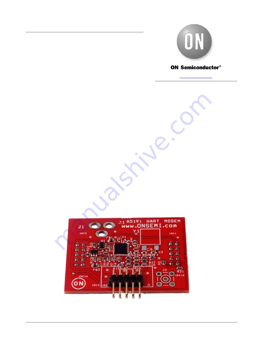
Figure 1. A5191HRTNGEVB Evaluation Board

www.onsemi.com

EVAL BOARD USER’S MANUAL

Summary of Contents for A5191HRTNGEVB

Page 1: ...t and transmit signal shaping The A5191HRT uses phase continuous frequency shift keying FSK at 1200 bits per second To conserve power the receive circuits are disabled during transmit operations and vice versa This provides the half duplex operation used in HART communications Features Single chip Half duplex 1200 Bits per Second FSK Modem Bell 202 Shift Frequencies of 1200 Hz and 2200 Hz 3 0 V 5 ...

Page 2: ...cillator and a modulator and demodulator module communicating with a UART without internal buffer The A5191HRT requires some external filter components and a 460 8 kHz clock source This clock source can either be the interface oscillator by using a crystal or ceramic resonator or an external clock signal When the device is transmitting data the receive module is shut down and vice versa to conserv...

Page 3: ...A5191HRTNGEVB www onsemi com 3 A5191HRTNGEVB DESCRIPTION Schematic Diagram Figure 2 Schematic of A5191HRTNEVB ...

Page 4: ...0603 3 R8 R16 R17 215k 0603 1 R12 1k 0603 1 R10 422k 0603 1 R13 3M 0603 1 R15 787k 0603 1 R18 24k 0603 1 R20 DNP 0603 Not populated 1 U1 CAT808NTDI 27GT3 ON Semiconductor 1 U2 A5191HRT ON Semiconductor 1 U3 TLV431ASNT1G ON Semiconductor 1 Y1 460 8 kHz ECS Crystal ZTBF 460 8 E General Overview The A5191HRTNGEVB evaluation board demonstrates the external components required for the operation of the ...

Page 5: ... mA IDD VDD 3 V Transmit 443 mA IDD VDD 3 V Receive 419 mA IDD VDD 6 V Transmit 837 mA IDD VDD 6 V Receive 781 mA IDD VDD 3 V Transmit Ext Osc 362 mA IDD VDD 3 V Receive Ext Osc 350 mA The module will use less power when clock signal is applied externally as this allows the modem to shut down the oscillator circuit As is to be expected a higher supply voltage increases current consumption It is ad...

Page 6: ...tage is recommended For A5191HRTNGEVB the TLV431 shunt regulator is used with an internal reference of 1 24 V This reference is compared against the output voltage and the shunt transistor base is adjusted until it sinks enough current to drop the output to 1 24 V A simple low pass filter formed by R12 and C11 is added to increase reference stability A slight voltage drop is observed over this fil...

Page 7: ...ors Alternatively a clock signal can be provided externally when R3 is removed and C3 is replaced by a resistor of 0 W This signal can be provided by a microcontroller or any other external oscillator circuit The module uses less power when clock signal is applied externally as this allows the modem to shut down the oscillator circuit A typical current consumption witnessed by utilizing an externa...

Page 8: ...ould be held low before any data is transmitted Data frames are not buffered by the modem Instead data is transmitted bit by bit Care should be taken to avoid clock skew in the receiving UART If the same time base is used for both the modem and the UART a 1 accurate time base may not be sufficient The problem is a combination of receive data jitter and clock skew between transmitting and receiving...

Page 9: ...a 0 W resistor The output on this pin is a 500 mVpp signal trapezoid waveform shown in Figures 10 and 11 This pin can only drive impedances higher than 30 kW and as a consequence may need to be amplified to drive low impedances For a given implementation of a master or slave it may be required to remove C4 and replace it with a 0 W resistor to allow the decoupling to occur elsewhere in the master ...

Page 10: ...the A5191HRTNGEVB The values are listed in Table 6 and the filter schematic is displayed in Figure 12 For cost purposes this filter can be implemented using E12 value resistors with minimal changes to the filter characteristic This implementation will have a slightly reduced gain in the pass band Figure 12 Receive Filter ...

Page 11: ...pF 5 Figure 13 Filter Characteristic First Stage black Total Blue In Figure 13 the simulated characteristic of the entire filter is shown in both variations for the first stage black and total filter blue The normal and low cost variations are superimposed showing that the variations are minimal However when the tolerance on the values is also loosened a bigger variation in the characteristic is o...

Page 12: ...an additional pole showing up at high frequencies This only improves the filter by rejecting high frequency noise and is too high in frequency to have an influence on the phase of HART signals Figure 16 shows the group delay of the total filter It is important that the difference in group delay between the mark and space is minimal so that the output of the filter still has coherence between both ...

Page 13: ... 17 This resembles the implemented filter except for the coupling capacitor on the operational amplifier and the removal of R14 The filter is a variation on the Sallen Key topology with three poles The AREF voltage serves here as a biasing voltage but can for ac frequencies be regarded as ground For a complete analysis of this filter type see the Appendix on Page 17 Figure 17 Simplified First Filt...

Page 14: ...nal transfer function of the first filter stage is thus a fourth order filter of the form The poles of this transfer function are located at p1 p2 195 Hz p3 1 220 kHz p4 22 kHz The input impedance of this filter stage is higher than 89 kW at frequencies below 50 kHz Figure 18 Input Impedance of the First Filter Stage Second Stage The second stage of the receive filter is a simple band pass filter ...

Page 15: ...rent flowing through the loop by changing the base of a transistor in emitter feedback configuration The value for R7 is determined by the output range Vo max of the amplifier used It is often recommended to take a value as large as possible so that noise effects are minimal Typically the value of R6 is chosen equal to R7 The voltage over R6 and R7 combined should however be less than 12 V when th...

Page 16: ...der To transmit a HART signal the TxA signal will need to be amplified as the A5191HRT transmit circuit can only drive high impedance circuits 30 kW An additional operational amplifier is required Depending on the sense resistor used some gain or attenuation may be required to get a 1 mA peak to peak HART output signal This can be accomplished by the resistors R3 and R4 For a typical sense resisto...

Page 17: ...similar to the one shown in Figure 17 We will derive the transfer function of this filter below We will denote the gain configured with RA and RB as K Resistors R3A and R3B serve only to bias the amplifier input in DC and can for the rest of the calculations be considered parallel and replaced by one resistor Using Kirkhof s current law we get in the three nodes of the filter eq 1 eq 2 eq 3 Solvin...

Page 18: ...tor on the operational amplifier results in the following transformation on the transfer function Where Since K is present in the numerator of the transfer function the zero of this factor will be present in the transformed transfer function The denominator of the transformed transfer function is a forth order function with the following coefficients The transfer function now has the following for...

Page 19: ...r results in the following transformation Since C3 is not present in the numerator or in the highest order coefficient no extra poles or zeros will be introduced by this transformation The form of the transfer function hence remains the same The transformed coefficients are ...

Page 20: ...liability arising out of the application or use of any product or circuit and specifically disclaims any and all liability including without limitation special consequential or incidental damages Buyer is responsible for its products and applications using ON Semiconductor products including compliance with all laws regulations and safety requirements or standards regardless of any support or appl...

Reviews: