background image

Summary of Contents for OMS-7

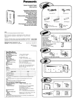
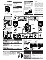
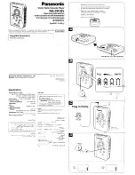
Page 1: ...Service Manual Nakamichi Nakamichi...

Page 2: ...e ene eene ee eel 17 7 5 Eject Load Switch P C B Ag Yi cees bi bee be Lvae sect etetevivenceuccnr en 17 7 6 Power Switch P C B Assy 2 eee cee cee cece enc eeeateeteenvecnn cee 17 7 7 MOMS PCBs ABSYa s...

Page 3: ...PICKUP REPLACEMENT PROCEDURES 2 1 Notice in Handling Pickup In case of repair or replacement of the Pickup pay attention to the following handling instructions since the laser diode in the Pickup is...

Page 4: ...ent of Pickup Upon completion of replacement of the Pickup perform rough adjustments following the flow chart shown in Fig 2 7 Then proceed to the final stage adjustment ie Adjustment Instructions in...

Page 5: ...e Disc 5A 8 Distortion Meter 6 Sony Test C D YEDS 7 4 PARTS LOCATION FOR ADJUSTMENT 4 1 Parts on P C B Ass y 8 b3000005 Main P C B CN201 D A Converter PC B RVSO1 Audio Signa Belonce RMOS 180n onsfifon...

Page 6: ...iled or defeated Avoid direct exposure to beam 1 Using Optical Power Meter a Unsolder one of the leads of diode D135 on the Main P C B Ass y b See Fig 5 1 Remove the Feed Motor Belt and with rotating...

Page 7: ...e Main P C B Ass y Short between the emitter and the base of Q113 on the Main P C B Ass y 4 Adjust VR102 to obtain 0 50 mV on the synchro scope 5 Remove the short of CN201 and Ql13 6 Connect the synch...

Page 8: ...tighten the Lock Screws alternately Tracking Screw Adjustment Test Disc Synchroscope Tracking Philips to TP1 TP6 emitter of Q103 on Main Main P C B P C B RV101 RVi02 RV103 RV104 Connect a synchroscop...

Page 9: ...0 wm scratch on and Dot on the test disc and listen to the playback sound Disc If playback is not made properly conduct step 6 Tracking Screw Adjustment Turn the Tracking Screw counterclockwise when t...

Page 10: ...n the following formula X 1 2 x 1 3 x Vpp 5 8 4 7 sensitivity of Tracking Servo 5 8 ohms DC resistance value of Traking Coil 4 7 ohms value of resistor R197 where 1 3 mm A If amount of eccentricity x...

Page 11: ...p Cover 0M04377A Caution Label A 0C80720A Vibration Isolating Sheet A Part No Description CA80287A Eject Load Switch P C B Ass y 0C81062A Vibration Isolating Sheet B 0C81063A 0C81063A 0C80721A 0C80722...

Page 12: ...l Ass y OMS 7 Front Panel Ass y OMS 7E Front Panel Ass y OMS 70 Front Panel OMS 7 Front Panel OMS 7E Front Panel OMS 70 Power Button Ass y Spring Side Frame L Sponge A R Skip Button F Skip Button Rev...

Page 13: ...Power Switch Sponge B Power Switch P C B Ass y P C B Bracket L Side Chassis L Damper Spring Disc Mechanism Ass y Hinge Center Chassis Main P C B Ass y D A Converter P C B Ass y Side Chassis R P C B Br...

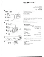
Page 14: ...6 4 Disc Mechanism Ass y B01 LO7 Fig 6 4 13 V01620 Druck 2...

Page 15: ...0947A 51 CA80236A 52 0C81158A 53 OC80969A 54 0C81004A 55 0C80974A 56 CA80353A 57 0C81002A 58 OC80992A 59 0C81016A 60 0C81022A 61 0C80773A 62 0C81020A 63 0C81018A 64 CA80282A 65 OC81017A 66 CA80281A 67...

Page 16: ...6 5 Rear Panel Ass y B02 H 3 Ss 07 LOS Others SS 03 DO1 6 6 Disc Mechanism Sub Ass y C01...

Page 17: ...ONailtap Screw 0C81342A M2 6x10 Pan OE00921A BT 3x8 Binding 0C81343A Bolt M3x12 Hex Socket Head Black Chromate 0C81344A Bolt M3x10 Hex Socket Head OE00818A M38x8 Binding Black Chromate 0C81346A Washe...

Page 18: ...ower Control P C B Transformer Alcan GES ooaeny o 1t o cE gel ge J ry JO00P500V a s oe ee aE QTo TPS60S ae J SO Ome eo eg rece Fig 7 1 bo 7 2 Photo Diode P C B Ass y Fig 7 6 oe DON TLNIO 4 2 Control P...

Page 19: ...0C81200A Photo Diode P C B Volume P C B 0B82341B XH Connector 3P LDO1 0C80759A Photo Diode OC81116A VR_ 10K A x2 700mm 1 TLN104 0C80857A 3P Connector 0B81282A Pin Jack 2P 1 Terminal 0C80919A CA80245A...

Page 20: ...ower Control P C B Ass y Feed Motor CA80241A 0C81174A Auto Power Control P C B UMO1 0C80923A IC BA4558 QM01 0C807438A TR 2SA1015 QM02 OC80756A TR 2SA794 DMO1 0C809382A ZD 8 2V MA1082 0C80877A4 SiD MA1...

Page 21: ...1K os aa SO RSIa RIS eee ag C3018 1 OO g 0 8 Moet SISOK i OK a ee aes 2216 3V 3F0 ino xt x 4 i a ocr on ee ae ge 9 28 Poa 50 aang a C30IA 4 R306C 10 1 Fig 7 13 Description See RF Pre Amp P C B C301A...

Page 22: ...BO1888A RKO5 OBO9645A RKO6 OBO1679A RKO8 OBO5579A RKO9 10 0B01706A 11 RK 10K 1 4WJ RK 47 1 6w J RK 100 1 4WJ RK 22 1 4w J RK 47 1 4wW J R112 212 O0B22596A RM 100K 1 4WF R113 114 0B22597A RM 300K 1 4WG...

Page 23: ...7 16 Analog Processor P C B Ass y 7 15 Control Switch P C B Ass y 206 IM teY to Main P C 8 CN208 300K G 7 16 Fig Fig 7 15 22...

Page 24: ...7 17 D A Converter P C B Ass y 534 0 022 541 9 oz2u 545 0 p 0 I oO o 8s a u506 4 700 a Og 1 AT 7 Fig oD nN...

Page 25: ...B41537A 0C80802A OB09993A OB05653A 0B41098A OB41176A 0B40159A 0B40063A 0B40076A 0B40088A 0C80804A O0C80836A O0C80837A 0C81134A 0C80829A CA80233A Description D A Converter P C B Ass y D A Converter P C...

Page 26: ...96 OBO5695A 312 313 R197 198 OBO97538A R199 251 OBO5698A R215 OB09924A R217 220 OB09548A R219 224 OBO5876A R232 235 OBO5675A R236 OBOS575A R237 238 0C81131A R243 0B05640A R246 OB09826A R247 OBO1887A R...

Page 27: ...7 18 Main P C B Ass y seanenpenangoconmi a RAQ a posi 26 V01620 Druck 3...

Page 28: ...verting Inverting Input A Input B V Non Inverting Input B TOP VIEW Fig 8 1 7 Operational Amp IC BA4558 LF353N 4560 Power Amp Pre Amp 3 Lay ts Ls 8 o 5s 2929 Oo 5 8 S oe 28 8 e By 8 8 a ge 96 ao Fig 8...

Page 29: ...INTO INT1 Interrupt R53 0 ORTI SCK SI SO Serial Interface R60 O O RTO DO 15 Bidirectional Ports R61 0 O R43 R00 03 60 63 70 73 80 83 R62 0 O R42 50 Output Ports R63 O O R41 SI R10 13 20 23 30 33 40 4...

Page 30: ...going pulse occurring at the end of each data frame nominal frequency 7 35 kHz Push pull output for symbol syne signal to the Error Corrector IC U504 A negative going pulse occurring during the last b...

Page 31: ...e PD2 ae Freq Fp 236 Detector OAI 169 OA2 179 OA3 18 vco2 219 8 64MHz vco vco 209 Register EFM Shift Decoder Register 27 DADE O26 L Timing Contro The data to the Error Corrector DADE consists of 32 x...

Page 32: ...n a subcoding sync word is detected Fig 8 1 16 Output Waveforms SAA7011 Description of Error Corrector IC U504 SAA7020 See Figs 8 1 17 and 8 1 18 Dota In Out Address Out DOER O7ER AOER AAER WEER OEFER...

Page 33: ...ta output between words on DAEC It is used to pass information with the data words A high on GAP making the GAP level on DAEC high and vice versa See Fig 8 1 18 39 SMSE In If SMSE is held low the UNEC...

Page 34: ...ut format a high selects 2 s complement a low offset binary see Fig 8 1 20 Note the data is descrambled internally so the input sample format is complex UNEC is the error flag input During the period...

Page 35: ...This muting attenuation occurs to data of left and right channels simultaneously regardless of the source of the mute The data good or processed is then formatted into 2 s complement or offset binary...

Page 36: ...eft channel test chain input See TINR eo ee Le TINR 15 TIN L ora Input OLCF Shift DRCF 17 Register Register CLCF 18 SIRE LY Timing Control CLOX 199 Bz TEST RT 22 TE 23 Fig 8 1 21 35 Pin Signal N 17 18...

Page 37: ...ccFO U507 6 DLFD ORFO U507 3 10 Fig 8 1 22 Input Output Waveform SAA7030 co oo a ane Shift Register Clock 280 O ieee ee Latch Enable 2 a VI 4 VIO 7 Decoupling v2 Il Binary Weighted Current Vref 3 Sou...

Page 38: ...Main P C B Ass y Warning Parts marked with the symbol have critical character istics Use ONLY replacement parts recommended by the manu facturer It is recommended that the unit be operated from a sui...

Page 39: ...Focus Serve Signal 2 H OPEN END en SWITCH P ee 5V O asoz Ri2q asciats 47K H 2SK246 2 cNM 05 ba cite ci7s TRACK NO TIME ye l 88 88 88 MEMORY INDEX NO DISC STAND BY REPEAT cN 208 Pouse a 58 fe PHOTO TRA...

Page 40: ...N 805 i hil Siz el N 209 Laser ra Li j2 3 s sjelt7 e afiofammfs fz i g ty CNM O7 CHM O3 g cLox qs s bal 2 paec U506 SAA7000 cq 4 CONCEA 2 8 UNEC 3 canons W807 84470280 selb a DIGITAL FILTER 3 3 22588...

Page 41: ...RY WHT clea afl ae aeaGLEE ieee sc ames e ee a ee ee z alee sfeoq eecced BLK BLK 8 19 cneog 1 CN203 CN204 cN205 a BLK cN2ot O6 Chassis eae aa BLK ep Chassis ae 3 Close End Switch P C B Assy Main P C B...

Page 42: ...8 _YELY l g 8 _REDY Power siege i a 5 8 ma Switch ps Vu Power Supply b z BRN z zee fk ea 5 Fig 10 _ pony dels L 313 BLU o 0000 cN208 ad CN206 uLeools 2 e IT a Ly i ome 15 4 cone bus WHT nfo s a see w...

Page 43: ...875A 0J04876A OJO4877A 0H04497B 0HO3920A 0E00941A OE00948A Remote Control Transmitter Unit Upper Case A Lens Remote Control Transmitter P C B Ass y Insu Lock Rubber Plate Upper Case B Terminal Plate A...

Page 44: ...10 Schematic Ref No LED602 Part No 0B12218A 0B06181A OB92001A R601 OB09925A 0B60118A Remote Control R602 OBO9677A Transmitter P C B C601 0B01836A OB11065A IC yuPD1943G C602 603 0B41079A 0B10049A TR 2S...

Page 45: ...n 0 003 1 kHz Channel Separation Better than 92 dB Output Line 2 V 1 kHz 0 dB 100 ohms Headphones 20 mW 1 kHz 0 dB output level control at max 8 ohms Power Source 100 120 120 220 240 220 or 240 V AC 5...

Page 46: ...Corporation 19701 South Vermont Ave Torrance CA 90502 Phone 213 538 8150 Nakamichi Canada 276 South West Marine Drive Vancouver B C V5X 2R4 Phone 604 324 7535 Nakamichi Australia Level 2 61A Dunning...

Reviews: