NAD T562, Service Manual
The NAD T562 Service Manual is essential for users seeking detailed instructions for troubleshooting and maintaining their device. This comprehensive manual is available for free download at manualshive.com, providing users with easy access to all the information they need to ensure optimal performance and long-lasting enjoyment of their NAD T562.
Share
Download


Reviews:
No comments
Related manuals for T562
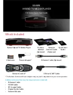
510 Series
Brand: KAMAI Pages: 8

8100 series
Brand: Califone Pages: 16

Fuze
Brand: SanDisk Pages: 38

RCD 930AX
Brand: Rotel Pages: 6

PDB1550
Brand: SOUNDMASTER Pages: 88

VC6001
Brand: Marantz Pages: 2

AZ1005
Brand: Philips/Magnavox Pages: 2

EZ season MX-110D
Brand: FUNAI Pages: 35

Joybee 120
Brand: BenQ Pages: 74

CMED3PRO
Brand: Conceptronic Pages: 148

TMP-3T
Brand: SDMC Pages: 31

C541
Brand: NAD Pages: 32

CVACC-E634
Brand: Chinavision Pages: 8

DMR-BWT700GL
Brand: Panasonic Pages: 10

DMR-UBS80EG
Brand: Panasonic Pages: 93

DMPBDT300 - 3D BLU-RAY DISC PLAYER
Brand: Panasonic Pages: 2

DMR-BWT460
Brand: Panasonic Pages: 80

DMR-UBC86
Brand: Panasonic Pages: 108


