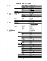
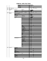
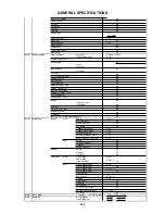
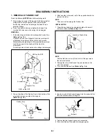
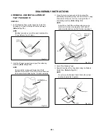
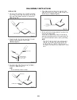
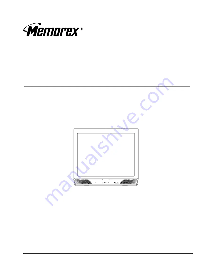
background image

SERVICE MANUAL

MT2327

Design and specifications are subject to change without notice.

COLOR TELEVISION  RECEIVER

ORIGINAL

MFR'S VERSION A

Summary of Contents for MT2327

Page 1: ...SERVICE MANUAL MT2327 Design and specifications are subject to change without notice COLOR TELEVISION RECEIVER ORIGINAL MFR S VERSION A ...

Page 2: ...hock while the electric current is flowing 3 USE THE DESIGNATED PARTS The parts in this equipment have the specific characters of incombustibility and withstand voltage for safety Therefore the part which is replaced should be used the part which has the same character Especially as to the important parts for safety which is indicated in the circuit diagram or the table of parts as a mark the desi...

Page 3: ...IC ELECTRICAL ADJUSTMENTS BLOCK DIAGRAM PRINTED CIRCUIT BOARDS MAIN CRT STEREO MAIN CRT SCHEMATIC DIAGRAMS MICON TUNER CHROMA DEFLECTION CRT POWER SOUND AV COMB FILTER AV JACK WAVEFORMS MECHANICAL EXPLODED VIEW MECHANICAL REPLACEMENT PARTS LIST ELECTRICAL REPLACEMENT PARTS LIST A2 1 A1 1 A1 1 A1 1 A2 1 A3 1 A3 4 B1 1 B2 1 B2 2 C 1 C 1 C 2 D 1 D 5 E 1 E 2 F 1 F 2 F 3 F 4 G 1 G 2 G 3 G 4 G 5 G 6 G 7...

Page 4: ...0V AC 60Hz DC Power Consumption at AC 130 W at AC 120 V 60 Hz Stand by at AC 5 W at AC 120 V 60 Hz Per Year kWh Year Protector Power Fuse Yes G 4 Regulation Safety UL CSA Radiation FCC IC X Radiation DHHS HWC G 5 Temperature Operation 5o C 40o C Storage 20o C 60o C G 6 Operating Humidity Less than 80 RH G 7 On Screen Menu Yes Display Menu Type Character Picture Yes Contrast Yes Brightness Yes Colo...

Page 5: ...Yes 4 Yes 5 Yes 6 Yes 7 Yes 8 Yes 9 Yes 0 Yes 100 No CH Up Yes CH Down Yes Volume Up Yes Volume Down Yes TV Caption Text Yes CH1 CH2 Yes TV Video TV AV Yes CH RTN CH ENT Quick View Yes Sleep Yes RE Call Call Yes Reset Yes Menu Yes Enter Yes Mute Yes Exit No MTS Audio Select Yes Set Yes Set Yes Multi Brand Keys CH Up VCR Yes CH Down VCR Yes Pause Still Yes TV VCR VCR Yes CH Enter Yes Code Set Code ...

Page 6: ... Brand No AC Cord No AV Cord 2Pin 1Pin No Registration Card No PTB Sheet No 300 ohm to 75 ohm Antenna Adapter No G 13 Interface Switch Front Power Yes System Select No Main Power SW No Sub Power No Channel Up Reset Yes Channel Down Enter Yes Volume Up Set Up Yes Volume Down Set Down Yes Menu Vol Up Vol Down Yes Rear AC DC No TV CATV Selector No Degauss No Main Power SW No Indicator Power No Stand ...

Page 7: ...e WHITE CORRUGATED CARTON Dimensions W x D x H mm 840 x 625 x 757 Design As per Buyer s Description of Origin Yes Drop Test Natural Dropping At 1 Corner 3 Edges 6 Surfaces Height cm 25 Container Stuffing 104 Sets 40 container G 17 Material Cabinet Cabinet Front PS 94V0 DECABROM Cabinet Rear PS 94V0 DECABROM PCB Non Halogen Demand No Eyelet Demand No A3 4 ...

Page 8: ...ip up the sides of the Rubber Cap in the direction of the arrow and remove one side of the support Refer to Fig 1 2 2 GND on the CRT Screwdriver Alligator Clip Support CRT GND on the CRT Rubber Cap CRT Support Fig 1 2 3 After one side is removed pull in the opposite direction to remove the other NOTE Take care not to damage the Rubber Cap INSTALLATION 1 Clean the spot where the cap was located wit...

Page 9: ... a blower type IC desoldering machine Refer to Fig 2 2 2 Fig 2 2 NOTE Do not add the rotating and the back and forth directions force on the IC until IC can move back and forth easily after desoldering the IC leads completely When IC starts moving back and forth easily after desoldering completely pickup the corner of the IC using a tweezers and remove the IC by moving with the IC desoldering mach...

Page 10: ...hin tip Soldering Iron NOTE When the IC leads are bent during soldering and or repairing do not repair the bending of leads If the bending of leads are repaired the pattern may be damaged So be always sure to replace the IC in this case Finally confirm the soldering status on four sides of the IC using a magnifying glass Confirm that no abnormality is found on the soldering position and installati...

Page 11: ...ITIAL DATA of MEMORY IC Refer to the WHEN REPLACING EEPROM MEMORY IC VOL MIN 8 Writing of EEPROM initial data NOTE Do not use this for the normal servicing VOL MIN Display of the Adjustment MENU on the screen Refer to the ELECTRICAL ADJUSTMENT On Screen Display Adjustment 9 POWER ON total hours can be checked on the screen Total hours are displayed in 16 system of notation NOTE If you set a factor...

Page 12: ...ess ENTER to select DATA When DATA is selected it will blink Again step through the DATA using SET or until required DATA value has been selected Pressing ENTER will take you back to ADDRESS for further selection if necessary Repeat steps 3 to 6 until all data has been checked When satisfied correct DATA has been entered turn POWER off return to STANDBY MODE to finish DATA input After the data inp...

Page 13: ...until the white color is looked like a white 1 2 3 4 5 6 7 8 2 5 VIF VCO Place the set with Aging Test for more than 15 minutes Receive an 80dB monoscope pattern Connect the digital voltmeter between the pin 5 of CP601 and the GND Activate the adjustment mode display of Fig 1 1 and press the channel button 03 on the remote control to select V VCO Press the VOL UP DOWN button on the remote control ...

Page 14: ...st to normal position Check if the step No V SHIFT is 0 Adjust the VR401 until the horizontal line becomes fit to the notch of the shadow mask Adjust the VR402 until the SHIFT quantity of the OVER SCAN on upside and downside becomes minimum D 2 2 9 VERTICAL SIZE 1 2 3 4 5 Receive the monoscope pattern Using the adjustment control set the brightness and contrast to normal position Activate the adju...

Page 15: ...e control to select SEP 1 Press the VOL UP DOWN button on the remote control to adjust it until the R ch output becomes minimum Set the multi sound signal generator L ch Non input R ch 1KHz and receive the RF Connect the oscilloscope to the pin 6 and pin 7 of CP601 Activate the adjustment mode display of Fig 1 1 and press the channel button 27 on the remote control to select SEP 2 Press the VOL UP...

Page 16: ...h the color bar generator from the green raster pattern to the crosshatch pattern Combine red and blue of the 3 color crosshatch pattern on the center of the screen by adjusting the pair of 4 pole magnets Combine red blue magenta and green by adjusting the pair of 6 pole magnets Adjust the crosshatch pattern to change to white by repeating steps 6 and 7 Turn the unit on and let it warm up for at l...

Page 17: ...CB R803 R805 J801 CP802B CP803B TP022 TP024 CP801 CP806 MAIN PCB CP802A CP1001 CP502 VR401 VR402 S501A FB401 T501 CP803A VR404 VR403 J707 J701 J705 TU001 CP601 S501B AC IN TP001 C P 4 0 1 CRT SPEAKER L 5 0 3 CRT VR502 TP401 D451 CD803 CD802 J702 J703 J704 STEREO PCB CD701 CP701 CD801 CP805 CD805 ...

Page 18: ...TE 51 AUDIO OUT VIF IN 1 G IN B IN R IN RF AGC OUT POWER ON CONT H OUT VREG Vcc VIF IN 2 20 SCL 26 SDA 27 10 V PULSE OUT 5 V OUT 28 FPB IN 14 DEGAUSS_H 13 15 STEREO 5V REG Q605 REG Q608 REG Q604 X602 3 579545MHz 31 11 49 8 7V REG OUT P CON 5 7V REG AT5 7V REG OUT Y SW OUT R OUT G OUT 47 28 RECTIFIER 16 B OUT Q606 REG REG Q603 AT 5V 3 4 6 5 2 REAR_AV IN STEREO J701 FEED BACK SW Q507 BUFFER Q502 SWI...

Page 19: ...45 C719 R749 D705 W025 Q706 R632 R629_1 Q608 Q606 W026 C628 Q604 Q605 C624 D601 D602 W027 IC702 HS1001 C1011 R1009 R1004 C1003 C1001 W031 D605 W114 C1008 W024 R621 W034 C1014 C003 C002 TP001 W107 W108 W109 C721 C706 C717 W093 W099 C707 W030 W037 W041 W112 W105 W110 W088 W137 W082 C1505 D1502 W092 C1527 R1520 W090 W049 Q1508 D1501 W050 C620 C645 W039 W102 W152 W171 R1003 W044 C630 C1009 R504 R1008 ...

Page 20: ...1517 R1504 C1518 R1506 C1516 R1517 C1519 C1523 R1508 R532 R533 R437 R534 R814 R816 R811 R815 R809 R813 C810 C809 C811 R808 R801 R810 C801 R817 R818 R819 C408 R722 R725 R726 R728 R723 R711 R709 R703 R704 R729 R727 R731 R710 C708 R622 R615 C602 R611 R004 C1004 R1014 R1015 C1002 R719 R1523 R1521 R1519 R1518 R110 R1002 R1006 R708 R505 R125 R133 R1511 R139 R102 R136 R643 C614 C1520 R143 R403 C110 C106 ...

Page 21: ...EES PAR UN ATTENTION DESCRIBED IN PARTS LIST ONLY CRITICAL FOR SAFETY USE ONES ARE SINCE THESE PARTS MARKED BY CAUTION D001 MTZJ30B D104 MTZJ6 8B Q103 KTC3198 BUFFER W801 TP001 W845 TM101 R25 1784 Q102 KTA1266 BUFFER L101 2 7uH Q101 KRC101MAT PROTECT SW IC199 S 24C08ADPA 01 MEMORY IC 1 2 3 4 5 6 7 8 SW101 SKHVBED010 32 CH UP SW103 SKHVBED010 32 VOL UP SW104 SKHVBED010 32 VOL DOWN SW105 SKHVBED010 ...

Page 22: ...S THE LATEST AT THE TIME DANS LA NOMENCLATURE DES PIECES N UTILISER QUE CELLS DECRITES DANGEREUSES AN POINT DE VUE SECURITE ETANT LES PIECES REPAREES PAR UN ATTENTION DESCRIBED IN PARTS LIST ONLY CRITICAL FOR SAFETY USE ONES ARE SINCE THESE PARTS MARKED BY CAUTION D610 MTZJ12B D611 MTZJ12B D612 MTZJ12B D607 MTZJ15B D602 MTZJ8 2B Q603 KTC3203_Y REG Q606 KTC3209_Y REG Q605 KTC3209_Y REG Q604 KTC3209...

Page 23: ...1 2W R440 220K 1 4W R443 4 7K 1 4W R437 2 7K R804 2 7K 1 4W R819 68 R810 220 R816 270 R818 68 R808 220 R813 270 R817 68 R806 2 7K 1 4W R801 220 R802 2 7K 1 4W R427 100 1 4W R445 39K 1 4W R441 4 7K 1 4W R438 10K 1 4W R458 680 1 2W R446 470 1 2W R444 22K 1 4W R404 220 1 4W R447_1 10K 1 4W R809 4 7K R814 4 7K R811 4 7K R405 1K 1 4W R459 820 1 2W R422 8 2K 1 2W R433 820 1 2W R416 1K 1 2W R415 560 1 2W...

Page 24: ...MHE C501 1000 35V YK R513 1K 1 2W R508 100 1 4W R512 270 1 4W R515 10K 1 4W R533 1K R532 820 R534 100 R514 6 8K 1 4W R505 10K R547 100 1 4W R516 100 1 4W R520 1 5M 1 2W R500 2 7M 1 2W 10 R503 1 2M 1 4W R511 1 2M 1 4W R507 150 1 4W R504 10K 1 2W R518 1K R555 100K 1 4W R554 27K 1 4W R535 68K 1 2W R536 68K 1 2W D523 1N4937 D521 1SS133 D516 1SS133 D505 30DF6 FC D502 RM11C EIC D503 RM11C EIC D510 RU 4A...

Page 25: ...ND SUBJECT TO CHANGE WITHOUT NOTICE NOTE THIS SCHEMATIC DIAGRAM IS THE LATEST AT THE TIME DANS LA NOMENCLATURE DES PIECES N UTILISER QUE CELLS DECRITES DANGEREUSES AN POINT DE VUE SECURITE ETANT LES PIECES REPAREES PAR UN ATTENTION DESCRIBED IN PARTS LIST ONLY CRITICAL FOR SAFETY USE ONES ARE SINCE THESE PARTS MARKED BY CAUTION W813 W864 W863 Q901 KTA1266 BUFFER Q902 KTA1266 BUFFER SCL SDA AUDIO_M...

Page 26: ...719 47 16V YK R707 1 2K R720 1K 1 4W R711 1K R709 1K R760 390 1 4W R702 10 1 4W R749 2 2K 1 4W R722 75 R723 75 R724 470 R731 2 2K R719 68 R703 1K R704 1K R708 82 R725 1 5K R727 4 7K R729 8 2K R726 1 8K R721 1K 1 4W R710 1 5K R728 1K OF PRINTING AND SUBJECT TO CHANGE WITHOUT NOTICE NOTE THIS SCHEMATIC DIAGRAM IS THE LATEST AT THE TIME D705 MTZJ12B Q705 KTC3198 MUTE Q707 KTC3198 MUTE Q701 KTC3198 BU...

Page 27: ...50V KA R1527 820 R1519 560 R1526 1K 1 4W R1503 2 2K R1501 390 R1506 820 R1504 100 R1505 100 R1521 180 R1512 10 R1515 27K R1514 27K R1517 1K R1508 560 R1520 1K 1 4W R1511 680 R1518 560 R1523 220 D1501 1SS133 D1502 1SS133 OF PRINTING AND SUBJECT TO CHANGE WITHOUT NOTICE NOTE THIS SCHEMATIC DIAGRAM IS THE LATEST AT THE TIME Q1507 KTC3199_Y BUFFER Q1502 KTC3199_Y BUFFER Q1505 KTC3199_Y BUFFER W866 W85...

Page 28: ... AND PICTURE IS NORMAL WITH THE DIGITAL TESTER WHEN THE COLOR BROADCAST NOTE THE DC VOLTAGE AT EACH PART WAS MEASURED C710 470P B C709 470P B C712 10 16V KA C713 10 16V KA C711 10 16V KA R701 82 1 4W R705 1K 1 4W R706 1K 1 4W OF PRINTING AND SUBJECT TO CHANGE WITHOUT NOTICE NOTE THIS SCHEMATIC DIAGRAM IS THE LATEST AT THE TIME TEBB05 PCB280 VIDEO GND AUDIO_R AUDIO_L AV JACK PCB AV JACK SCHEMATIC D...

Page 29: ...s were measured at the point of the corresponding balloon number in the schematic diagram CHROMA 1 1V 0 1µs div 6 0 5V 20µs div 200mV 20µs div 7 9 200mV 20µs div 0 5V 5ms div 10 8 20V 20µs div 11 1V 20µs div 12 1V 20µs div 1V 20µs div 13 DEFLECTION CRT 14 0 5V 5ms div 15 20V 20µs div 29 500mV 200ns div ...

Page 30: ...onding balloon number in the schematic diagram H 2 200V 20µs div 17 22 50V 20µs div 50V 20µs div 20 10V 5ms div 19 21 50V 20µs div SOUND 25 0 5V 1ms div 26 200mV 1ms div 200mV 1ms div 27 10V 5ms div 18 28 200mV 1ms div 16 2V 20µs div 31 200mV 1ms div 0 5V 1ms div 32 0 5V 1ms div 33 ...

Page 31: ...1 201 206 116 112 104 205 115 115 117 117 106 V801 107 207 207 117 117 107 J801 PCB110 CRT PCB ASS Y 207 207 110 108 202 202 202 202 118 102 PCB280 STEREO JACK PCB ASS Y 101 111 109 SP1002 204 113 SP1001 204 113 204 119 119 119 203 204 203 203 203 103 114 203 105 203 203 ...

Page 32: ...LT SHEET 150x5 T 0 3 116 800WQ0A002 FELT SHEET 5x130xT0 5 117 762WPA0009 HOLDER CRT WIRE 118 735WPA0694 STOPPER BUTTON 119 800WQ00041 FELT SHEET 390x18xT0 5 201 8109I30A04 SCREW TAP TITE B WH7 3x10 202 8110630A24 SCREW TAP TITE P BRAZIER 3x12 203 8117540B04 SCREW TAPPING B0 TRUSS 4x20 204 8110630A04 SCREW TAP TITE P BRAZIER 3x10 205 8109630802 SCREW TAP TITE B BRAZIER 3x8 206 8107630804 SCREW TAP ...

Page 33: ... IC M62420FP C501 E02LF4102M CE 1000 UF 35V IC401 I03TD80410 IC LA78041 C505 P2122B224M CMP 0 22 UF 250V ECQUL or IC402 I1KJ98L090 IC KIA78L09BP AT P2472B224M CMP 0 22UF 275V PHE840 IC501 0002E00610 PHOTO COUPLER LTV 817M VB C506 P2122B104M CMP 0 1 UF 250V ECQUL or IC601 I06FC61250 IC M61250FP P2472B104M CMP 0 1 UF 275V PHE840 IC702 I0QS02245L IC NJM2245L C507 E51CGC471M CE 470 UF 200V IC901 I01FF...

Page 34: ...03A L608 021LA66R8K COIL 6 8 UH TU001 0145100059 TUNER VHF UHF ENV56DB6G3 L701 021LA6270K COIL 27 UH V801 0981320603 CRT W DY M80LNK185X90Y1 L801 02167D470K COIL 47 UH X602 100CT3R505 CRYSTAL HC 49 C L901 021375101K COIL 100 UH or 02167D101K COIL 100 UH RESISTOR L1501 02167F101J COIL 100 UH RC CARBON RESISTOR L1502 02167F101J COIL 100 UH L1503 021LA6100J COIL 10 UH CAPACITORS L1504 021LA6150J COIL...

Page 35: ...M3M0 02N O R NO SPEC NO W273017 ...

Reviews: