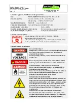
background image

DRS

Series

All-in-one Multi-function Security Power Supply

User Manual

+

+

+

+

Back-up

Charger

Power Supply

DRS 240 480

-

/

Series

AC Grid

Load

Battery Pack

Modbus

RTU

DATA

PROTOCOL

AC

DC

Summary of Contents for DRS Series

Page 1: ...DRS Series All in one Multi function Security Power Supply User Manual Back up Charger Power Supply DRS 240 480 Series AC Grid Load Battery Pack Modbus RTU DATA PROTOCOL AC DC ...

Page 2: ...rse polarity protection The DRS series also provides Form C contacts and LED indicators as alarm signals for AC fail battery low charger circuit fail and DC OK allowing easy integration into security systems This series has 2 stage and 3 stage charge curves selectable by DIP switch charging curves can also be programmed by SBP 001 as well as manual adjustment through a potentiometer ADJ on the pan...

Page 3: ...tion 4 2 Pin assignment 4 3 LED indicator 5 Explanation of Setting 5 1 DC voltage supply 5 2 DC UPS 5 3 Battery charging 5 4 Communication monitoring function 5 5 Alarm signals 5 6 Battery Start by Battery Start Button Content 5 7 Battery Start by Force Button 5 Battery temperature 8 compensation 5 9 P boost ower mode 5 Restore actory 10 f d s efault etting 6 Protection and Failure Correction 6 1 ...

Page 4: ... is suitable for lead acid batteries flooded water type gel colloid type AGM adsorption glass fibber or lithium ion lithium manganese lithium ternary etc Note 1 Pollution Degree 2 applies where there is only non conductive pollution that might temporarily become conductive due to occasional condensation Generally refer to dry well ventilated locations such as control cabinets 2 2 l All In One Inte...

Page 5: ...rent limiting power will shutdown after 5 sec re power on to recover Combined power on all Channels must not exceed 240W load has priority 275W peak capability within 5s 2 4 DRS 480 Series 480mVp p 48V 93 5 41 8 1V DRS 480 48 0 10A 105 135 rated output power MODEL OUTPUT VOLTAGE Note 2 OUTPUT LINE REGULATION LOAD REGULATION HOLD UP TIME Typ VOLTAGE RANGE FREQUENCY RANGE POWER FACTOR Typ EFFICIENCY...

Page 6: ...0 80 100 Horizontal 20 0 15 30 0 40 50 30 60 70 2 Pending 6 2 6 Mechanical Specification DRS 240 Series V V V V N L BAT BAT 129 2 85 5 125 2 TB1 TB3 TB4 1 2 3 4 5 6 7 8 9 101112 1 2 3 4 1 2 3 Charging Current Adj AC Fail DC OK Status Battery Start 4 2 6 8 3 1 5 7 CN12 ON 2 1 3 1 8 TB2 1 2 3 4 Communication Port RJ45 Unit mm 2 ...

Page 7: ...rt ON 2 1 3 1 8 4 2 6 8 3 1 5 7 CN12 Communication Port RJ45 Unit mm 2 8 3 Installation Wiring 3 1 Installation Methods Admissible DIN rail TS35 7 5 TS35 15 35 Tilt the unit slightly rearwards Fit the unit over top hat rail Slide it downward until it hits the stop Press against the bottom for locking Shake the unit slightly to check the locking action 1 2 3 4 5 3 only for reference not included in...

Page 8: ...0V 105 12 3 3 22 10 5 3 35 7 10 46 6 16 60 4 25 80 Recommendations for the use of wires 10 Models 12V 24V 36V 48V D RS 240 20 200AH or above 10 100AH 6 6 66 AH 5 50AH D RS 480 20 200 AH 13 133AH 10 100AH 3 4 Battery Selection Battery types Lead acid or lithium ion batteries Battery capacity Please refer to the following table Battery capacity recommendation NOTE 1 Using batteries with greater capa...

Page 9: ... cm 8Kgf cm 10 22AWG 8Kgf cm 10 22AWG 2Kgf cm 16 26AWG Cable selection and suggested torque 4 2 Pin Assignment PIN definition of CN12 JS 2008R 4 2 T or equivalent Open Normal Short Force Pin 3 Function 4 RTH RTH 1 2 3 3V GND 5 A0 6 A1 7 8 Terminal Pin No Assigment TB4 Terminal Pin No Assigment RJ 45 Pin 1 2 3 4 5 6 Function AC fail Charger fail 7 8 9 10 11 12 DC OK Battery low Abnormal Disconnecte...

Page 10: ... Optional models Charger Fail Bat Bat Battery AC Input RJ45 SBP 001 smart programmable Personal Computer 1 8 DC OK Communication Port Modbus communication Standard models RJ45 1 8 Communication Port RS 485 Personal Computer RJ45 USBCAN Personal Computer 1 8 Communication Port CAN Optional models Bus communication DRS series integrates multi functions in tiny dimension including DC output power bat...

Page 11: ...itial stage of charging the charger charges the battery with the maximum current and the fan is ON built in fan model After a period of time depending on the battery capacity the charging current gradually decreases When the charging current drops to 10 of the rated current LED indicator lights up in green indicating that the charging process is complete If the charging is finished power supply wi...

Page 12: ...LiFeO4 2 OFF OFF OFF ON ON ON OFF OFF OFF ON ON ON 3 OFF OFF OFF OFF OFF OFF ON ON ON ON ON ON Vboost Vboost Vboost 7 7A 5 1A 3 85A 43 2 57 6 42 56 0 42 6 56 8 43 8 58 4 24V model 36V model 48V model 2 3 2 3 28 8 28 0 28 4 29 2 2 OFF ON OFF ON 3 OFF OFF ON ON Vboost 15 4A 12V model 14 4 14 0 14 2 14 6 2 OFF OFF OFF ON ON ON OFF OFF OFF ON ON ON 3 OFF OFF OFF OFF OFF OFF ON ON ON ON ON ON 2 3 2 3 N...

Page 13: ... 001 1 2 UART_RX PMBUS_D CANH 5V 3 3V UART_TX PMBUS_C CANL GND GND 9 10 LED 5V Orange 3 3V Green Personal Computer SBP 2 1 2 10 9 DRS 480 Communication cable Smart programmer by another request To the personal computer USB port 20 5 This device supports Modbus RTU with the master salve principle During data transfer please follow the principle of first sending the High byte and then the Low byte e...

Page 14: ...us Slave ID is set by CN12 A0 A1 The device address is set as follows 22 5 5 4 1 5 Function Code Description The main purpose of the function codes is to tell the slave what kind of action to perform For example function code 03 will query the slave to read holding registers and respond the master server with their contents Function Code of DRS as follow Read Holding Register Read Input Register P...

Page 15: ...ta description Refer to transmission data description Refer to transmission data description Refer to transmission data description 24 5 0x00B4 CURVE_CONFIG Configuration setting only for charger 0x00B5 CURVE_CC_TIMEOUT CC charge timeout setting only for charger Min 0x00B6 CURVE_CV_TIMEOUT CV charge timeout setting 0x00B7 CURVE_FV_TIMEOUT FV charge timeout setting only for charger 0x00B8 2 CHG_STA...

Page 16: ...f a certain model is 0 01 the communication reading value is 0x0960 hexadecimal 2400 decimal then Vo_real 2400 0 01 24 00V Reserved Lowbyte HI_TEMP OP_OFF AC_FAIL SHORT OLP OVP OTP FAN_FAIL 26 5 0x4D 0x4C 0x45 0x4C 0x41 0x20 0x4E 0x20 0x57 0x20 0x45 0x20 Byte 0 Byte 0 Byte 1 Byte 1 Byte 2 Byte 2 MFR_ID_B0B5 MFR_ID_B6B11 Byte 3 Byte 3 Byte 4 Byte 4 Byte 5 Byte 5 MFR_ID_B0B5 0x0080 0x0082 is the fir...

Page 17: ... R 0x the MCU number 2 is 01 3 0D version R 0x the MCU number 3 is version R01 0x0 01 2 0C 1 B the MCU number version R01 0x0 other s are 0 A 0x0A 0x0A Byte 4 Byte 5 0x0D 0x0C 0x0B 0x0A Byte 0 Byte 1 Byte 2 Byte 3 28 5 Low byte Bit 0 1 CUVS Charge Curve Selection 00 Customized charge curve default 01 Gel battery 10 Flooded battery 11 AGM battery Bit 2 3 TCS Temperature Compensation Setting 00 disa...

Page 18: ...g of buffering 0 NO time out in buffering 1 Buffering time out Reserved Reserved Reserved Reserved Reserved Bit7 Bit6 Bit5 Bit4 Bit3 Bit2 Bit1 Bit0 High byte FVTOF CVTOF CCTOF BUFFTOF BTNC NTCER Low byte FVM CVM CCM FULLM CHG_STATUS 0x00B8 only for charger DCM 30 5 Bit 5 CCTOF Time out flag of constant current mode 0 NO time out in constant current mode 1 Constant current mode time out Bit 6 CVTOF...

Page 19: ...4 0 001 0x5 0 01 0x6 0 1 0x7 1 0 0x8 10 0x9 100 0xA 0xF Reserved Reserved Reserved Reserved Reserved Reserved IIN Factor CURVE_TIMEOUT Factor TEMPERATURE_1 Factor FAN_SPEED Factor VIN Factor VOUT Factor 32 5 Byte1 Bit 0 3 VIN Factor The factor of AC input voltage 0x0 Not support AC input relevant commands 0x1 0x3 Currently not in use retain default is 0 0x4 0 001 0x5 0 01 0x6 0 1 0x7 1 0 0x8 10 0x...

Page 20: ...Secondary DC output voltage status 0 Secondary DD output voltage status TOO LOW 1 Secondary DD output voltage status NORMAL Bit 2 PFC_OK Primary side PFC output voltage status Not support 0 Primary side PFC no starting or abnormal 1 Primary side PFC normal Bit 3 ORING_OFF ORING MOS OFF Not support 0 DD start up ORING MOS controller ON 1 DD start up force control ORING MOS OFF Bit 4 ADL_ON Active d...

Page 21: ...4 2 Communication examples The following provides examples of request and response for each function code of the Modbus RTU 5 4 2 1 Read Holding Register FC 03 The request message specifies the starting register and quantity of registers to be read Request 0x83 0x03 0x00 80 0x00 06 0xDA 02 0x83 Slave ID 3 0x03 Function code 3 Read analog output holding R registers 0x00 80 The data address of the f...

Page 22: ...he request message specifies the register reference to be written For example the master writes PSU ON to analog output holding register of 0x0000 OPERATION for slave 3 The normal response is an echo of the query returned after the register contents have been written Response 38 5 5 4 3 CANBus communication l Physical layer This protocol complies with CAN ISO 11898 and baud rate is 250Kbps l Proto...

Page 23: ...R W 40 5 Constant current setting format value F 0 01 Constant voltage setting format value F 0 01 Floating voltage setting format value F 0 01 Taper current setting format value F 0 01 0x00B0 CURVE_CC 2 R W 0x00B1 CURVE_CV 2 0x00B2 C URVE_FV 2 0x00B3 CURVE_TC 2 R W R W R W 0x00B4 CURVE_CONFIG 2 Configuration setting R W Manufacture serial number Manufacture serial number 0x0087 MFR_SERIAL_B0B5 6 ...

Page 24: ... of READ_VOUT of a certain model is 0 01 the communication reading value is 0x0960 hexadecimal 2400 decimal then Vo_real 2400 0 01 24 00V 5 42 5 Bit1 Bit0 OTP Bit7 Bit6 Bit5 Bit4 Bit3 Bit2 Low byte OP_OFF AC_FAIL SHORT OLP OVP Low byte Bit 0 FAN_FAIL Fan abnormal state Not support 0 Normal state 1 Abnormal state Bit 1 OTP Over temperature protection 0 Normal internal temperature 1 Abnormal interna...

Page 25: ...0 0x0086 is manufacture date ASCII EX MFR_DATE_B0B5 is meaning 2018 01 01 180101 MFR_SERIAL_B B5 MFR_SERIAL_B6B11 0 0x0087 0x0088 are defined as manufacture date and manufacture serial number ASCII EX The first unit manufactured on 2018 01 01 MFR_SERIAL_B0B5 180101 000001 MER_SERIAL_B6B11 0x30 0x31 Byte 4 Byte 5 0x30 0x31 Byte 4 Byte 5 0x30 0x31 Byte 4 Byte 5 0xFE 0x69 0x0A 0xFF Byte 0 Byte 1 Byte...

Page 26: ...G_STATUS 0x00B8 only for charger DCM 46 Low byte Bit 0 FULLM Fully charged mode status 0 NOT fully charged 1 Fully charged Bit 1 CCM Constant current mode status 0 The charger NOT in constant current mode 1 The charger in constant current mode Bit 2 CVM Constant voltage mode status 0 The charger NOT in constant voltage mode 1 The charger in constant voltage mode Bit 3 FVM Float mode status 0 The c...

Page 27: ..._OK Secondary DC output voltage status 0 Secondary DD output voltage status TOO LOW 1 Secondary DD output voltage status NORMAL Bit 2 PFC_OK Primary side PFC output voltage status Not support 0 Primary side PFC no starting or abnormal 1 Primary side PFC normal Bit 3 ORING_OFF ORING MOS OFF Not support 0 DD start up ORING MOS controller ON 1 DD start up force control ORING MOS OFF Bit 4 ADL_ON Acti...

Page 28: ... Bit6 Bit5 Bit4 Bit3 Bit2 Bit1 Bit0 Reserved Reserved Reserved Reserved Reserved Reserved Reserved Reserved Reserved Reserved Reserved Reserved Reserved 5 Time_ UPS_ OFF_EN Life_ Test_EN f_EN Buf 50 CANBus Modbus Command Model Range Tolerance 0x0050 READ_VIN ALL 80 305V 2V 0x0060 READ_VOUT 12V 0 15V 0 12V 24V 0 30V 0 24V 0 45V 0 36V 0 60V 0 48V 0x0061 READ_IOUT DRS 240 12V 0 20A 0 2A 24V 0 10A 0 1...

Page 29: ... 48V AC OK HL SET _ _ _ ALL 137 187V 182 6Vac 0x00E4 TIME BUFFERING _ ALL 60 64800 minute 5 minute 5V 5V 5V 24V 36V 48V 24V 36V 48V 0 2A 0 066A 0 05A 0 13A 0 2A CURVE_FLOAT_TI 600 minute 5 52 5 5 Alarm Signals 1 L or AC Fail DC OK Battery ow Relays of Charger Fail will be triggered according to different abnormal condition 2 An external voltage source is needed and maximum voltage is 30Vdc and sin...

Page 30: ...BAT BAT TB1 TB3 TB4 1 2 3 4 5 6 7 8 91011 12 1 2 3 4 1 2 3 Charging Current Adj AC Fail DC OK Status Battery Start 4 2 6 8 3 1 5 7 CN12 ON 2 1 3 1 8 TB2 1 2 3 4 Communication Port RJ45 5 6 1 Short press the Battery Start button to connect to the battery to start the mode 5 6 2 Long pressing the Battery Start button for 3sec can release the connection from the battery to deactivate the mode 5 6 3 B...

Page 31: ...mperature sensor NTC Bat Bat Batter y AC Input 8 pins JS 2008R 2 4 T RTH RTH NTC According to customer s request 56 5 8 2 No compensation if temperature sensor disconnected Only Lead acid batteries can use this compensation 5 8 1 CANBus and Modbus commands can modify parameters of temperature compensation There are four selections Disable 3mV Cell 4mV Cell and 5mV Cell and default setting is 3mV C...

Page 32: ... Load Do not exceed 6 minutes in 10 minute cycle When maxim output current double rated current um draw s the the output period is 4 minutes and 4 seconds at triple maximum current draw 10A 20A 30A power power power BAT BAT BAT max 4min max 4sec Output power 58 5 Load 30A 2s 2s 2s 20A 10A time 0 10 min Do not exceed 6 seconds in 10 minute cycle 5 10 Restore Factory Default Setting User can reset t...

Page 33: ...If battery under voltage protection is triggered by force button please refer to 5 7 3 60 6 2 Failure Correction Status Possible cause Suggestion for fault correction Battery can not be fully charged Aged battery or malfunction Small cross section of cable Wrong charging curve Change new batteries Choose a proper cable for usage Double check the characteristic of battery Note 1 Refer to chapter 4 ...

Page 34: ...ase refer to the latest version of our manual on our website https www meanwell com MEAN WELL WEB User s Manual This product provides three years warranty under normal usage Do not replace parts or any form of modification to the product in order to keep the warranty effectively 7 62 ...

Page 35: ...59 No 28 Wuquan 3rd Rd Wugu Dist New Taipei City 248 Taiwan ...

Reviews: