background image

Mini Hi-Fi System

SERVICE MANUAL

MODEL: RAT376B 

(RAS376BF/W)


CAUTION

BEFORE SERVICING THE UNIT, READ THE “SAFETY PRECAUTIONS”
IN THIS MANUAL.

MODEL: RAT376B (RAS376BF/W)

SERVICE MANUAL

P/NO : AFN74972241

JANUARY, 2011

Website http://biz.lgservice.com

Internal Use Only

Summary of Contents for RAS376BF

Page 1: ...MANUAL MODEL RAT376B RAS376BF W CAUTION BEFORE SERVICING THE UNIT READ THE SAFETY PRECAUTIONS IN THIS MANUAL MODEL RAT376B RAS376BF W SERVICE MANUAL P NO AFN74972241 JANUARY 2011 Website http biz lgservice com Internal Use Only ...

Page 2: ...CONTENTS SECTION 1 GENERAL SECTION 2 CABINET MAIN CHASSIS SECTION 3 ELECTRICAL SECTION 4 REPLACEMENT PARTS LIST 1 1 ...

Page 3: ...SECTION 1 SUMMARY CONTENTS SERVICING PRECAUTIONS 1 3 ESD PRECAUTIONS 1 5 SERVICE INFORMATION FOR EEPROM 1 6 PROGRAM DOWNLOAD GUIDE 1 7 SPECIFICATIONS 1 9 1 2 ...

Page 4: ... the eyes Absolutely never permit laser beams to enter the eyes Also NEVER switch ON the power to the laser output part lens etc of the pick up if it is damaged 5 Cleaning the lens surface If there is dust on the lens surface the dust should be cleaned away by using an air bush such as used for camera lens The lens is held by a delicate spring When cleaning the lens surface therefore a cotton swab...

Page 5: ...eplacing a component part first disconnect the power supply lead wire from the unit 2 All equipment measuring instruments and tools must be grounded 3 The workbench should be covered with a conductive sheet and grounded When removing the laser pick up from its conductive bag do not place the pick up on the bag This is because there is the possibility of damage by static electricity 4 To prevent AC...

Page 6: ... damage ESD devices 5 Do not use freon propelled chemicals These can generate electrical charges sufficient to damage ESD devices 6 Do not remove a replacement ESD device from its protective package until immediately before you are ready to install it Most replacement ESD devices are packaged with leads electrically shorted together by conductive foam aluminum foil or comparable conductive materia...

Page 7: ...ate position and make changes with remote control skip mode play key Press STOP key FLD write ok Remote control Fwd skip Front STOP push same timing FLD E2P CLR Completed NAME OPT0 OPT1 OPT2 OPT3 OPT4 OPT5 OPT6 OPT7 OPT8 OPT9 DETECT NEW EEPROM OPTION EDIT SCREEN HEX 05 00 00 00 00 08 80 06 50 08 1 6 SERVICE INFORMATION FOR EEPROM ...

Page 8: ...wnload the file to your set Caution When downloading the file you should neither unplug the USB device change to the other function nor power off the device USB device must be unplugged when the downloading process is completed ON VFD DISPLAY SCREEN NO USB Insert USB device at USB function READ FIRMWARE WRITE 00 100 UPDATED POWER OFF AUTOMATICALLY When completed remove USB device 1 7 PROGRAM DOWNL...

Page 9: ...ftware then download the file to your set Caution When downloading the file you should neither unplug the usb device change to the other function nor power off the device USB device must be unplugged when the downloading process is completed ON VFD DISPLAY SCREEN NO USB Insert usb device at USB function READ FIRMWARE WRITE 00 100 FINISH POWER OFF AUTOMATICALLY When completed remove USB device 1 8 ...

Page 10: ...e 87 5 to 108 0 MHz or 87 50 to 108 00 MHz FM Intermediate Frequency 128 kHz AM Tuning Range 522 to 1 620 kHz 520 to 1 710 kHz or 522 to 1 710 kHz AM Intermediate Frequency 45 kHz AMPLIFIER Stereo mode 110 W 110 W 4 Ω at 1 kHz THD 10 Surround mode Front 110 W 110 W 4 Ω at 1 kHz THD 10 Subwoofer 150 W 3 Ω at 60 Hz THD 10 CD Frequency response 40 Hz 20 kHz Signal to noise ratio 75 dB Dynamic range 8...

Page 11: ...1 10 MEMO ...

Page 12: ...SECTION 2 CABINET MAIN CHASSIS CONTENTS EXPLODED VIEWS 2 3 1 CABINET AND MAIN FRAME SECTION RAT376 2 3 2 MECHANISM DECK SECTION CDM 345 2 5 3 PACKING ACCESSORY SECTION 2 7 4 SPEAKER SECTION 2 8 2 1 ...

Page 13: ...2 2 MEMO ...

Page 14: ...FRONT MAIN USB SMPS 260L 460 460 261 460 460 264 451 A47 276 265 259 A26 460 460 A46 300 460 460 273 274 460 CABLE2 260R A43 A44 460 A42 460 251 NOTES THE EXCLAMATION POINT WITHIN AN EQUILATERAL TRIANGLE IS INTENDED TO ALERT THE SERVICE PERSONNEL TO THE PRESENCE OF IMPORTANT SAFETY INFORMATION IN SERVICE LITERATURE ...

Page 15: ...6 2 5 2 2 MECHANISM DECK SECTION CDM 345 018 439 014 013 017 019 026 015 020 A01 A02 001 002 003 016 036 010 012 012A 012A 432 432 037 A03 A26 MEMO 431 012 ...

Page 16: ...2 7 825 FM Wire Antenna 824 AM Loop Antenna 900 Remote Control 803 Packing 808 Battery 802 Box 801 Instruction Ass y 804 Bag 3 PACKING ACCESSORY SECTION ...

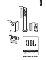
Page 17: ...2 8 A60 4 SPEAKER SECTION 4 1 FRONT SPEAKER RAS376BF ...

Page 18: ...2 9 A90 4 2 PASSIVE SUBWOOFER RAS376BW ...

Page 19: ...2 10 MEMO ...

Page 20: ...ER AUX FUNCTION CHECK 3 25 8 TUNER FUNCTION CHECK 3 26 CDP ELECTRICAL TROUBLESHOOTING GUIDE 3 27 1 CD FUNCTION 3 27 2 USB FUNCTION 3 28 WAVEFORMS 3 29 WIRING DIAGRAM 3 33 BLOCK DIAGRAMS 3 35 1 OVERALL BLOCK DIAGRAM 3 35 2 SMPS BLOCK DIAGRAM 3 37 CIRCUIT DIAGRAMS 3 39 1 SMPS CIRCUIT DIAGRAM 3 39 2 MICOM AD CIRCUIT DIAGRAM 3 41 3 PWM AMP CIRCUIT DIAGRAM 3 43 4 CD DSP SERVO CIRCUIT DIAGRAM 3 45 5 FRO...

Page 21: ...bleshoot Countermeasure 1 Check if the fuse F901 is open or short circuit 2 Check if the bridge diode DB901 is short circuit by over current with a digital multi meter 3 Check if the NTC thermistor TH901 is normal or open 1 1 3 Service hint Any picture Remark F901 If F901 is not short circuit replace it with a same specifications one TH901 If TH901 is open replace it with a new one BD901 If BD901 ...

Page 22: ...2 D929 1 2 1 Solution Please check and replace D929 on SMPS board 1 2 2 How to troubleshoot Countermeasure 1 Check the Anode Cathod Voltage of D929 with a digital multi meter it is normally 0 2 0 3 V If it doesn t have any voltage it s destroyed Replace it with a new one 1 2 3 Service hint Any picture Remark SMPS schematic diagram ...

Page 23: ... Check 3 7 V to CN304 and CN105 in standby mode If there is no 3 7 V check the SMPS 2 Check 5 6 V 12 V F F and PVDD when power on the set If the set doesn t work regardless of what the KEY1 changes high to low while pressing the power button X101 and X102 work normally but if you can not power on the set replace IC101 with a new one on the MAIN board 2 1 3 Service hint Any picture Remark w y j ys ...

Page 24: ...SMPS to VFD via the MAIN board 2 Check if IC102 outputs VFD_D0 VFD_CLK and VFD_STB to the FRONT board 3 Check the GR signal pulse signal of IC501 on the FRONT board Check the SG signal pulse signal of IC501 on the FRONT board If the GR and SG signal isn t output replace IC501 with a new one If the GR and SG signal is output replace DIG502 with a new one 3 1 3 Service hint Any picture Remark znG ny...

Page 25: ...PDO signal from pin16 of IC302 If no signal check 3 3 V RF and X301 2 Check the SPIN SPIN from IC301 to CN303 for driving SPINDLE motor It is about 3 6 Vp p If no signal check 1 8 V and 5 V for IC301 3 Check if the FFC cable is solidly connected between CN303 and MD 4 Check the MD If the spindle motor is sort circuit or has any trouble it can not rotate CD discs Please check the function after cha...

Page 26: ...15 of IC302 If no signal check 3 3 V RF and X301 2 Check the SLED SLED from IC301 to CN303 for driving SPINDLE motor It is about 2 9 Vp p If no signal check 1 8 V and 5 V for IC301 3 Check if the FFC cable is solidly connected between CN303 and MD 4 Check the MD If the sled motor is sort circuit or has any trouble it can not move the pickup module Please check the function after changing another M...

Page 27: ... If no signal check 1 8 V 5 V to IC301 2 Check LOAD from IC301 to CN303 for driving the tray open close motor It is about 3 85 Vp p If no signal check 5 V to IC301 If it has any trouble replace it with a new one 3 Check if the FFC cable is solidly connected between CN303 and MD 4 Check the MD If the tray motor is sort circuit or has any trouble it can not open or close the tray Please check the fu...

Page 28: ... positioned in the center of a track on CD disc 1 Check the TRD signal from Pin14 of IC302 If no signal check 3 3 V RF and X301 2 Check TR TR from IC301 to CN301 for driving the tracking actuator If no signal check 1 8 V and 5 V for IC301 3 Check if the FFC cable is solidly connected between CN301 and MD 4 Check the MD If the pickup module has any trouble it can not move the laser beam on the left...

Page 29: ...a regular interval with the surface of a CD disc 1 Check the FOD signal from Pin13 of IC302 If no signal check 3 3 V RF and X301 2 Check F F from IC301 to CN301 for driving the focusing actuator If no signal check 1 8 V and 5 V for IC301 3 Check if the FFC cable is solidly connected between CN301 and MD 4 Check the MD If the pickup module has any trouble it can not move the laser beam on the top o...

Page 30: ...llowing I2S signal flow I2S audio signal Interface DAC_BCK IC801_Pin87 IC602_Pin4 DAC_LRCK IC801_Pin88 IC602_Pin5 44 1 kHz DAC_DATA IC801_Pin83 IC602_Pin6 9 DAC_MCLK IC801_Pin86 IC401_Pin44 If there is any trouble check the power for each IC The power is normal but if the signal waveform to the IC is distorted or no signal replace it with a new one 3 Check if Digital audio AMP block on Item 5 2 is...

Page 31: ...602 Refer to I2S audio signal interface on Item 5 1 2 Check PVDD If PVDD is abnormal check the SMPS 3 Check 12 V for driving the gate of AMP IC a All the powers are normal but if 12 V is low there is possible for AMP IC to be damaged b Remove L711 L712 L713 and L714 one by one When removed a inductance if 12 V is recovered AMP IC connected to it was damaged c Replace AMP IC with a new one 4 Check ...

Page 32: ...N501 2 Check USB D from MAIN board to USB board a Check USB_DN DP signals to IC801 pin116 117 b Check USB signals from IC504 to CN501 pin2 3 If there is any trouble check the power for each IC The power is normal but if the signal waveform to the IC is distorted or no signal replace it with a new one 3 Check if Digital audio AMP block on item 5 2 is normal 5 3 3 Service hint Any picture Remark kT ...

Page 33: ...e it a new one 4 Check the following I2S signal flow from IC801 to IC602 Refer to Item 5 1 If there is any trouble check the power for each IC The power is normal but if the signal waveform to the IC is distorted or no signal replace it with a new one 5 Check if the digital audio AMP block is okay Refer to Digital Audio AMP guide on Item 5 2 If AMP is damaged replace it with a new one 5 4 3 Servic...

Page 34: ... ADC_DATA is entered from IC401 to IC801 If no signal check 5 V 3 3 V ADC for IC401 If is NG replace it a new one 4 Check the following I2S audio signal flow from IC801 to IC602 Refer to Item 5 1 If there is any trouble check the power for each IC The power is normal but if the signal waveform to the IC is distorted or no signal replace it with a new one 5 Check if the digital audio AMP block is o...

Page 35: ...upplied to IC901 Pin7 Is D904 normal YES NO Check or replace D904 Is there about 2 5 V at IC903 Pin1 Replace IC903 YES NO Is D923 normal Replace D923 YES NO Is D921 normal Replace D921 YES NO Is D924 normal Replace D924 YES NO Is D925 normal Replace D925 YES NO Is D922 normal Replace D922 YES NO Power line of I O PCB is short NO 3 16 AUDIO ELECTRICAL TROUBLESHOOTIHG GUIDE ...

Page 36: ... V supplied to IC902 Pin7 Is D905 normal YES NO Check or replace D905 Check P CTRL H signal from μ COM Check PC902 Is Q902 normal Replace Q902 Check or replace Q910 YES NO Is D929 normal Replace D929 YES NO Is there about 2 5 V at IC904 Pin1 Replace IC904 YES NO Is Q910 base H Power line of main PCB is short NO NO 3 17 AUDIO ELECTRICAL TROUBLESHOOTIHG GUIDE ...

Page 37: ...13 V Supplied to Q953 base Check P CTRL H signal from μ COM YES NO Check or replace Q953 No 5 V Is Vcc 6 V supplied to IC951 Pin1 Check or replace D923 YES YES NO Check IC951 Pin4 H Check P CTRL H signal from μ COM YES NO Check or replace IC951 3 18 AUDIO ELECTRICAL TROUBLESHOOTIHG GUIDE ...

Page 38: ...FD Is D925 normal Check or replace D925 YES YES NO Is ZD951 normal Is Q951 normal Check or replace ZD951 Check or replace Q951 YES YES NO NO Check or replace VFD 3 19 AUDIO ELECTRICAL TROUBLESHOOTIHG GUIDE ...

Page 39: ...heck if IC102_Pin49 and IC102_Pin36 59 are 3 5 V YES Check D102 D105 Replace D102 D105 NO NO X101 32 768kHz X102 9 8304MHz Check the operation OK YES YES YES YES YES OK 3 IC101 S24CS16A01 CHECK CHECK IC102 PIN47 48 Refer to μ COM troubleshooting NO Pin47 DATA Pin48 CLK Replace μ COM NO YES Check μ COM voltage 3 5 V Check μ COM YES OK OK YES YES NO 3 20 AUDIO ELECTRICAL TROUBLESHOOTIHG GUIDE ...

Page 40: ...Check CN304 connection YES Check each Pin voltage YES Check IC501 ET6315 voltage Pin30 VKK 26 V Pin13 43 5 V YES Check IC102 IC501 data communication Pin3 Pin9 STB Pin2 Pin7 DATA Pin4 Pin8 CLK FLD light on OK NO If voltage is Not 3 7 VA check input and output of D501 YES Check IC501 YES NO Replace IC501 NO Check input data IC102 Pin2 3 4 YES OK Check IC102 YES NO Replace IC102 Check output data IC...

Page 41: ...2 MHz NO Refer to SMPS troubleshooting Check X602 19 2 MHz operation NO Replace X602 19 2 MHz Check X602 19 2 MHz OK YES NO Check IC602 PS9850 Pin51 CLK input Check IC102 LC87Fxx Pin41 PWM RESET Pin45 PWM SDA Pin46 PWM SCL output NO Replace R636 R637 R638 Check line resistor output RST R636 SCL R637 SDA R638 NO YES YES YES YES YES YES OK YES A 3 22 AUDIO ELECTRICAL TROUBLESHOOTIHG GUIDE ...

Page 42: ...eck CD Assy communication Pin4 5 6 OK NO NO Check each line resistor output Check IC602 PS9850 input data Check PWM modulator output FL Pin31 30 FR Pin28 27 and others NO Replace IC602 PS9850 Check IC602 PS9850 NO OK YES YES YES YES YES YES A 3 23 AUDIO ELECTRICAL TROUBLESHOOTIHG GUIDE ...

Page 43: ...C701 Pin30 31 38 39 42 43 50 51 input voltage YES Check each line resistor output voltage NO Check each IC603 Pin64 12 V input Check IC701 IC702 Pin28 29 36 37 43 44 52 53 Replace the coil NO Check output line coil Check PWM Modulator input IC700 Pin4 5 10 11 IC701 Pin4 5 YES YES YES YES OK 3 24 AUDIO ELECTRICAL TROUBLESHOOTIHG GUIDE ...

Page 44: ...401 CS5346 Pin9 output data YES Check IC401 Pin5 5 V Pin46 3 3 V Check CN105 Pin7 5 V Pin9 10 3 3 V NO NO Check IC801 MLC9800 input data YES Check IC401 Pin5 5 V Pin6 High Pin46 3 3 V Check IC401 Pin41 SDOUT Pin42 SLCK Pin43 LRCK Pin44 MCLK NO NO IC501 MLC9800 output data OK YES 3 25 AUDIO ELECTRICAL TROUBLESHOOTIHG GUIDE ...

Page 45: ...ON CHECK Check tuner module voltage Pin4 3 3 V NO Check tuner module TU100 operation YES YES Check IC102 Pin21 22 23 24 25 data in output Check tuner module data NO YES Refer to function check 3 26 AUDIO ELECTRICAL TROUBLESHOOTIHG GUIDE ...

Page 46: ...eck the signal 16 0344 MHz of IC302 Pin31 NO YES Check IC801 input output and control line NO YES YES Check loading motor NO OPU driving Focus and tracking is ok NO Focus tracking sled signal is ok NO Check IC301 Motor drive IC NO Is the PD CN301 Pin12 about 180mV YES Check Vcc of IC302 Check Cristal X301 NO Replace Cristal X301 Replace IC801 Check IC301 YES 1 CD FUNCTION Check OPU pick up NO 3 27...

Page 47: ...502 YES Plug in usb device Check CN401 NO NO YES Display READ YES Display NO FILE YES Check usb jack JK501 NO Replace IC801 NO Check IC801 Pin116 117 Check usb audio file in usb device MP3 WMA file is playable YES 2 USB FUNCTION 3 28 CDP ELECTRICAL TROUBLESHOOTIHG GUIDE ...

Page 48: ...1 SDRAM 1 2 3 4 CLK DATA ADDRESS CS 2 SERVO 5 CD 16M 3 29 WAVEFORMS IC802 Pin38 IC802 Pin53 IC802 Pin35 IC803 Pin1 IC801 Pin63 ...

Page 49: ...FE TE FOD RF 6 7 8 9 3 AUDIO PATH 10 11 12 CD_BCK CD_LRCK CD_DATA 3 30 IC302 Pin61 IC302 Pin62 IC302 Pin63 IC302 Pin13 IC801 Pin100 IC801 Pin102 IC801 Pin101 ...

Page 50: ...13 14 16 15 DAC_MCK DAC_BCK DAC_LRCK DAC_DATA 4 USB 17 USB_5V D D 18 3 31 IC801 Pin86 IC801 Pin87 IC801 Pin88 IC801 Pin83 IC801 Pin116 IC801 Pin117 ...

Page 51: ...3 32 MEMO ...

Page 52: ...3 33 3 34 6PIN CDM 345 CN301 CN303 CN302 CN105 CN401 CN501 CN304 CN104 CN502 CN902 CN903 CN901 WIRING DIAGRAM ...

Page 53: ... s Fs Ts SPINDLEs LOAD s TDO SLDO SPDO FDO 12MHZ 16 93MHZ MLC9800 MCS LOGIC RESET MU TE POWER I F 3 7V 12V VFD DRIVER ET6315 AUX DAT CLK RST CE INT RST WEN CE A 0 18 DB 0 15 OP CL OP CL LI MIT CD BCK LRCK DOUTA DAC MCLK P SENSE MICOM LC87F5M64A PWM PS9850 DO STB CLK ADC CLK ADC DAT ADC RST ADC DATA TUNER R L R L I2S CLK DAC BCK LRCK MCLK DAC DATA 12 288MHZ PWM RST PWM CLK PWM DAT PDN SD OTW FL FL ...

Page 54: ...MPS IC Block T R A N S Snubber Block م م Photo coupler Photo coupler Photo coupler FL FL On Off Vkk On Off 5V 5V LDO 12V 12V Regulation Block 3 7VA P CTL On Off On Off م م م م م م م م AMP SMPS IC With FET Block م F U S E Y Cap Y Cap م T R A N S SMPS م 5 6VA CD P CTL CN901 CN902 3 Feedback Feedback ...

Page 55: ...IT USED THIS WAY IMPLEMENTATION OF THE LATEST SAFETY AND PERFORMANCE IMPROVEMENT CHANGES INTO THE SET IS NOT DELAYED UNTIL THE NEW SERVICE LITERATURE IS PRINTED NOTE 1 Shaded parts are critical for safety Replace only with specified part number 2 Voltages are DC measured with a digital voltmeter during Play mode A 1 2 3 4 5 6 7 8 9 10 11 12 B C D E F G H I J K L M N O P Q R S T CAUTION Danger if f...

Page 56: ...3 41 3 42 2 MICOM AD CIRCUIT DIAGRAM A 1 2 3 4 5 6 7 8 9 10 11 12 B C D E F G H I J K L M N O P Q R S T µ COM AD EBY61070801 1 Rev 1 9 2010 11 09 ...

Page 57: ...3 43 3 44 3 PWM AMP CIRCUIT DIAGRAM A 1 2 3 4 5 6 7 8 9 10 11 12 B C D E F G H I J K L M N O P Q R S T PWM AMP EBY61070801 2 Rev 1 9 2010 11 09 ...

Page 58: ... 46 4 CD DSP SERVO CIRCUIT DIAGRAM 10 12 11 17 18 15 14 13 16 3 1 2 4 8 5 7 6 9 A 1 2 3 4 5 6 7 8 9 10 11 12 B C D E F G H I J K L M N O P Q R S T CD DSP SERVO EBY61070801 3 Rev 1 9 2010 11 09 WAVEFORM NUMBER ...

Page 59: ...3 47 3 48 5 FRONT CIRCUIT DIAGRAM A 1 2 3 4 5 6 7 8 9 10 11 12 B C D E F G H I J K L M N O P Q R S T FRONT EBY61070901 Rev 2 2 2010 11 09 ...

Page 60: ...3 49 3 50 6 USB CIRCUIT DIAGRAM A 1 2 3 4 5 6 7 8 9 10 11 12 B C D E F G H I J K L M N O P Q R S T USB EBY61071001 Rev 1 5 2010 11 09 ...

Page 61: ... 0 41 3 22 0 41 32 VDD_IO 2 97 3 63 3 22 0 41 3 22 0 41 35 VDD_IO 2 97 3 63 3 24 0 39 3 24 0 39 40 VDD_IO 2 97 3 63 3 24 0 39 3 24 0 39 Location Pin No Specification EE Mode V Margin Playback Mode V Margin 43 VDD_CORE 1 08 1 32 1 24 0 08 1 24 0 08 48 VDD_IO 2 97 3 63 3 22 0 41 3 22 0 41 57 VDD_CORE 1 08 1 32 1 24 0 08 1 24 0 08 59 VDDA 1 08 1 32 1 24 0 08 1 24 0 08 61 VDD_VIN2 2 20 3 30 3 22 0 08 ...

Page 62: ...12 74V C408 100uF 16V 0V 0V 0V 16V 2 49V 0V 2 49V 13 51V 0 0 0V 16V C410 47uF 16V 0 24V 0V 0 24V 15 76V 4 97V 0V 4 97V 11 03V 3 65 0 3 65V 12 35V C423 47uF 16V 0V 0V 0V 16V 4 02V 0V 4 02V 11 98V 1 41 0 1 41V 14 59V C613 10uF 16V 0V 0V 0V 16V 1 25V 0V 1 25V 14 75V 1 24 0 1 24V 14 76V C6A0 470uF 10V 0V 0V 0V 10V 1 25V 0V 1 25V 8 75V 1 24 0 1 24V 8 76V C6A1 100pF 50V 0 18V 0V 0 18V 49 82V 1 65V 0V 1 ...

Page 63: ...3 55 3 56 PRINTED CIRCUIT BOARD DIAGRAMS 1 MAIN P C BOARD TOP VIEW Rev 2 2 ...

Page 64: ...3 57 3 58 MAIN P C BOARD BOTTOM VIEW EAX63554401 Rev 2 2 ...

Page 65: ...3 59 3 60 2 SMPS P C BOARD 3 FRONT P C BOARD Rev 6 2 NOTE Warning Parts that are critical with respect to risk of fire or electrical shock ...

Page 66: ...3 61 3 62 4 USB P C BOARD MEMO ...

Page 67: ...3 63 3 64 MEMO MEMO ...

Reviews: