TK-7102
TK-7102
© 2001-5 PRINTED IN JAPAN
B51-8584-00 (S) 283
VHF FM TRANSCEIVER
TK-7102
SERVICE MANUAL
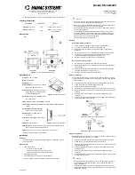
Panel assy
(A62-0942-03)
Front glass
(B10-2668-03)
Cabinet
(A01-2178-02)
Key top
(K29-9065-01)
SPECIFICATIONS
GENERAL
Frequency Range ................................ 146 to 174MHz
Number of Channels ........................... 4 channels
Channel Spacing ................................. Wide : 25kHz
Narrow : 12.5kHz
PLL Channel Stepping ........................ 2.5, 5, 6.25, 7.5kHz
Operating Voltage ............................... 13.6V DC ±15%
Current Drain ...................................... Less than 0.4A on standby
Less than 1.0A on receive
Less than 8.0A on transmit
Operating Temperature Range ........... –30°C to +60°C
Dimensions & Weight ........................ 160 (W) x 43 (H) x 107 (D) mm, Approx 1.0kg
Channel Frequency Spread ................ 28MHz
RECEIVER
(Measurements made per EIA standard EIA/TIA-603)
Sensitivity (12dB SINAD) .................... Wide : 0.28µV
Narrow : 0.35µV
Selectivity ........................................... Wide : 75dB
Narrow : 65dB
Intermodulation ................................... Wide : 70dB
Narrow : 60dB
Spurious Response ............................. 75dB
Audio Power Output ........................... 4.0W
Frequency Stability ............................. ±2.5ppm
TRANSMITTER
(Measurements made per EIA standard EIA/TIA-603)
RF Power Output ................................ 25W
Spurious and Harmonics ..................... 70dB
Modulation .......................................... Wide : 16K0F3E
Narrow : 11K0F3E
FM Noise ............................................ Wide : 45dB
Narrow : 40dB
Audio Distortion .................................. Less than 3%
Frequency Stability ............................. ±2.5ppm
KENWOOD CORPORATION
14-6, Dogenzaka 1-chome, Shibuya-ku, Tokyo 150-8501, Japan
KENWOOD SERVICE CORPORATION
P.O. BOX 22745, 2201 East Dominguez Street, Long Beach, CA 90801-5745,
U.S.A.
KENWOOD ELECTRONICS CANADA INC.
6070 Kestrel Road, Mississauga, Ontario, Canada L5T 1S8
KENWOOD ELECTRONICS DEUTSCHLAND GMBH
Rembrücker Str. 15, 63150 Heusenstamm, Germany
KENWOOD ELECTRONICS BELGIUM N.V.
Mechelsesteenweg 418 B-1930 Zaventem, Belgium
KENWOOD ELECTRONICS FRANCE S.A.
13, Boulevard Ney, 75018 Paris, France
KENWOOD ELECTRONICS U.K. LIMITED
KENWOOD House, Dwight Road, Watford, Herts., WD1 8EB United Kingdom
KENWOOD ELECTRONICS EUROPE B.V.
Amsterdamseweg 37, 1422 AC Uithoorn, The Netherlands
KENWOOD ELECTRONICS ITALIA S.p.A.
Via G. Sirtori, 7/9 20129 Milano, Italy
KENWOOD IBERICA S.A.
Bolivia, 239-08020 Barcelona, Spain
KENWOOD ELECTRONICS AUSTRALIA PTY. LTD.
(A.C.N. 001 499 074)
16 Giffnock Avenue, Centrecourt Estate, North Ryde, N.S.W. 2113, Australia
KENWOOD ELECTRONICS (HONG KONG) LTD.
Unit 3712-3724, Level 37, Tower one Metroplaza, 223 Hing Fong Road, Kwai Fong, N.T.,
Hong Kong
KENWOOD ELECTRONICS TECHNOLOGIES(S) PTE LTD.
Sales Marketing Division
1 Ang Mo Kio Street 63, Singapore 569110