background image

70%

MD PERSONAL STEREO SYSTEM

MDX-F1

SERVICE MANUAL

P

U

SH OPEN

0

FM 75

AM

GND

AC IN 

ANTENNA

In compliance with Federal Regulations, following are
reproductions of labels on, or inside the product relating to
laser product safety.

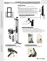
* Refer to parts list on page 40 .

KENWOOD-Crop. certifies this equipment conforms to
DHHS Regulations No.21 CFR 1040. 10, Chapter 1, Sub-
chapter J.

DANGER : Laser radiation when open and interlock
d e f e a t e d .  
AVOID DIRECT EXPOSURE TO BEAM.

Front glass
(B10-3540-04)

Knob ass'y
(K29-7753-04) : S
(K29-7755-04) : R

Panel ass'y
(A60-1729-02) : S
(A60-1803-02) : R

Knob
(K29-7669-02)

Front glass
(B10-3541-03)

Knob
(K29-7669-02)

Knob
(K29-7718-03) : S
(K29-7750-03) : R
Cassette holder
(A53-2174-02) : S
(A53-2188-02) : R

Rod antenna
(T90-0828-05)

Plastic cabinet
(A02-2949-01) : S
(A02-2950-01) : R

Lock terminal board
(E70-0051-05)

Miniature phone jack
(E11-0399-05)

Panel
(A29-1078-04)

S : silver

R : red

Note: Please contact KENWOOD service in your side if
you want to get the AC power cord.

Summary of Contents for MDX-F1

Page 1: ...GER Laser radiation when open and interlock defeated AVOID DIRECT EXPOSURE TO BEAM Front glass B10 3540 04 Knob ass y K29 7753 04 S K29 7755 04 R Panel ass y A60 1729 02 S A60 1803 02 R Knob K29 7669 02 Front glass B10 3541 03 Knob K29 7669 02 Knob K29 7718 03 S K29 7750 03 R Cassette holder A53 2174 02 S A53 2188 02 R Rod antenna T90 0828 05 Plastic cabinet A02 2949 01 S A02 2950 01 R Lock termin...

Page 2: ...s made to record a 256th track An attemptis made to assign a titlewith more characters than usable The disc does not contain any record ings The disc does not contain any tracks but has a disc title The TOC 1 data of the disc is being read The data related to editing or recording is being writtenin the disc The contentsof UTOC 2 are abnormal An attempt is made to perform editing beyond the restric...

Page 3: ... MD EDIT indication LOUD Loudness indication EX BASS extra bass indication TITLE SEARCH MHz kHz O T E TAPE EQ STEREO TUNED AUTO TOTAL 3ALL 3REPEAT 3RANDOM SLEEP TRACK NO PM AM FM 8 8 8 8 8 8 8 8 MD EDIT 1 2 LOUD EX BASS A P S O T T PROG REC REC PGM 5 6 7 2 4 1 0 3 3 9 8 Cassette holder POWER key STANDBY TIMER indicator Remote sensor Display STOP key CD MD TAPE TUNING MODE key CD MD TAPE tuner tuni...

Page 4: ...e 8 screws on rear panel 2X8 3 Remove 3 screws on rod ant 3X3 4 Lift rear side of top cover and remove it Insert the screw driver to contact of door ass y and sub panel if remove door ass y How to Disassemble Front Panel and Rear Panel How to Remove Door Ass y 5 Remove 4 screws 4X4 6 Lift and slide CD parts of top cover by using handle 7 Remove 6 long screws 5X6 slide front panel front wards ...

Page 5: ...Hz 22 FM 76 00MHz 37 FM 76 00MHz 23 FM 76 00MHz 38 FM 76 00MHz 24 FM 76 00MHz 39 FM 108 00MHz 25 FM 76 00MHz 40 AM 945kHz BAND RECEIVING CHANNEL IF PLL FREQ SPACE FM 76 0MHz 87 5MHz 100kHz 10 7MHz 25kHz FM 87 5MHz 108MHz 50kHz 10 7MHz 25kHz AM 531kHz 1629kHz 9kHz 450kHz 9kHz ACTIVE Port Port Name I O Descriptions H L 1 DSTP O CD disc motor servo control output port OFF ON 2 XLON O Bias control por...

Page 6: ...cancel control port ON OFF 70 BIAS O Bias control port ON OFF 71 CPM O Cassette deck motor control port ON OFF 72 SOL O Cassette deck solenoid control port ON OFF 73 PLAY SW I Cassette deck play switch control port OFF ON 74 CrO2 SW I CrO2 tape detection CrO2 NORMAL 75 PACK SW I Cassette half switch control port OFF ON 76 REC F I Cassette deck forward rec switch control port OFF ON 77 REC R I Cass...

Page 7: ...NSE signal form MD LSI input port 25 PDOWN I Power down detection port 26 HDON O Current control of record head 27 EEPROM O Cancel signal output port to EEP ROM 28 4 23 O 4 23MHz 29 EEPK O EEP ROM serial clock port 30 EEPD I O EEP ROM data I o port 31 MDDATA O MD data output port 32 KDATA I System data input port 33 DSCK I System synchro clock input port 34 DSTB O System line busy or to permit usa...

Page 8: ... GND 97 NC O No use 98 VREF I 3 2V 99 AVCC I 3 2V 100 PR I GND In Tape Mode 4 seconds recording mode only FTC Sub clock Oscillation a Check the oscillation yes or no period before FTC test mode b Check is 5 times by 200ms FTC test mode is carried out if one time is OK c Display shows error message as follows and test mode will be stop No oscillation î ERR 1 Poor period î ERR 2 7 2 Cancel a Cancel ...

Page 9: ...value FG value Both TG and FG values 09 FE value RF value Both FE and RF values 10 TE value VC value Both TE and VC values SKIP UP EX 01 02 CD s track up operation MD REC Time CD s FF operation Feed the pickup outwards at STOP mode SKIP DOWN EX 02 01 CD s track down operation TAPE REC Time CD s FB operation Feed the pickup inwards at STOP mode Value shows self adjustment result and hex 7 4 3 MD Mo...

Page 10: ...rfectly however not write AUTO pre adjustment Carry out AUTO pre adjustment and write data to EEPROM NG_EEPROM Not write the data of setting values Check the connection of MD microprocessor and EEPROM Carry out the TEST PLAY TEST REC and C1 error in test mode after AUTO_ADJ and AUTO_FAB 7 4 4 MD SECTION 1 2 Test disc Type Test disc 1 High reflection disc TGYS1 SONY 2 Low reflection disc Recording ...

Page 11: ...EJECT mode TEMP setting of EEPROM setting 1 AUTO pre adjustment mode Low reflection disc only Step No Setting Method Remarks Display Step 1 Testmode STOP state t s m e Step 2 Press once the MD REC button AUTO pre adjustment menu AUT_ YOBI_ _ _ Step 3 Press once the MD PLAY button The slide moves to the innermost periphery and automatic _ _ _ _ _ _ _ pre adjustment is started During automatic adjus...

Page 12: ...1 Press once the MD REC button Indication of measurement value S E G _ _ _ Step 12 Press once the MD REC button Indication of measurement value S F G _ _ _ Step 13 Press once the MD REC button Indication of measurement value H A O _ _ _ Step 14 Press once the MD REC button Indication of measurement value H B O _ _ _ Step 15 Press once the MD REC button Indication of measurement value H E O _ _ _ S...

Page 13: ...ing EFMIO measurement g M I _ _ _ Step 20 Press once the MD REC button RF side pit section FG adjustment R F G _ _ Step 21 Press once the MD REC button Focus ATT A signal setting S A G Step 22 Press once the MD REC button Focus ATT B signal setting S B G Step 23 Press once the MD REC button Offset 0 setting A signal offset measurement H A O _ _ _ Step 24 Press once the MD REC button B signal offse...

Page 14: ...8 Press once the MD REC button Focus ATT A signal setting L A g Step 9 Press once the MD REC button Focus ATT B signal setting L B g Step 10 Press once the MD REC button Outside periphery move Track closs setting G C G Step 11 Press once the MD REC button Tracking ATT E signal setting G E G Step 12 Press once the MD REC button Tracking ATT F signal setting P F G Step 13 Press once the MD REC butto...

Page 15: ...C W ERR Error of writing to UTOC WRITING In writing to UTOC 8 MD mechanism error message Display Value Voltage TOC recording power Actual power output 00H 2 50 mW 6E H 1 354 V 01H 2 60 mW 74 H 1 427 V 02H 2 70 mW 7B H 1 513 V 03H 2 85 mW 83 H 1 612 V 04H 3 00 mW 8A H 1 698 V 05H 3 15 mW 93 H 1 809 V 06H 3 30 mW 93 H 1 809 V 07H 3 45 mW 9C H 1 920 V 08H 3 60 mW A6 H 2 043 V 09H 3 75 mW AE H 2 141 V...

Page 16: ... O2 6X e MI e J YeN e 7 H e e f e f e f e 3 L e Le N XeJ e 3 KO Ye V4 0R Y e W g W g W g Y g g g g g g g g g g g g f W 2 6Kf O e M I Le He N 1e f e f e f e f 5e Le J He K O e V4 0Mf h h h h h g O2 6Kf MI e J YeV Le 7 H e N 1e g e g e 3 L e J e N XeW e KO e I4 0Y 5e J He W 5 e W Y e O Yf O2 0Y f 0M g O2 6Kf MI e J YeV Le 7 H e N 1e g e g e 3 L e J e N XeW e KO e I4 0Y 5e J He W 5 e W Y e O Yf O2 0Y...

Page 17: ... V4 0M f W2 6T 7 eI L V 3 Kf V 6Xe V4 X I 1 N XeJ KO 5 R4 0Y W e W e e N e e O2 6X e MI e J YeN e 7 H e e f e f e f e 3 L e Le N XeJ e 3 KO Ye V4 0R Y e W g W g W g Y g g g g g g g g g g g g f W 2 6Kf O e M I Le He N 1e f e f e f e f 5e Le J He K O e V4 0Mf h h h h h g O2 6Kf MI e J YeV Le 7 H e N 1e g e g e 3 L e J e N XeW e KO e I4 0Y 5e J He W 5 e W Y e O Yf O2 0Y f 0M g O2 6Kf MI e J YeV Le 7 ...

Page 18: ...5 f 7 Y f J Yg W Y g W Yh W Y fO e W Ye 0Y e e e O2 6X f Xf J MeI 1f Y e N f f f J 5f 7 Hf J 5 f 7 Y f J Yg W Y g W Yh W Y fO e W Ye 0Y e O2 6X f Xf J MeI 1f Y e N f f f J 5f 7 Hf J 5 f 7 Y f J Yg W Y g W Yh W Y fO e W Ye 0Y e W g W g W g Y g g g g g g g g g g g g f W2 6Xf W MI X e 7 HeN 1 e J 5 e 3 Le 7 H e N 1e g e g e g e g e g e g e 3 L e J 5e N 1 e 7 He 3 LeJ 5 e V KO Y e V4 0Yf e e e e W2 e ...

Page 19: ... J H e K O e V 4 0 M f h h h h h g O 2 6 K f M I e J Y e V L e 7 H e N 1 e g e g e 3 L e J e N X e W e K O e I 4 0 Y 5 e J H e W 5 e W Y e O Y f O 2 0 Y f 0 M g O 2 6 K f M I e J Y e V L e 7 H e N 1 e g e g e 3 L e J e N X e W e K O e I 4 0 Y 5 e J H e W 5 e W Y e O Y f O 2 0 Y f 0 M g e e W g W g W g Y g g g g g g g g g g g g f O 2 6 X f X f J M e I 1 f Y e N f f f J 5 f 7 H f J 5 f 7 Y f J Y g W...

Page 20: ... g g g g g g g f W 2 6Kf O e M I Le He N 1e f e f e f e f 5e Le J He K O e V4 0Mf h h h h h g O2 6Kf MI e J YeV Le 7 H e N 1e g e g e 3 L e J e N XeW e KO e I4 0Y 5e J He W 5 e W Y e O Yf O2 0Y f 0M g O2 6Kf MI e J YeV Le 7 H e N 1e g e g e 3 L e J e N XeW e KO e I4 0Y 5e J He W 5 e W Y e O Yf O2 0Y f 0M g e e W g W g W g Y g g g g g g g g g g g g f O2 6X f Xf J MeI 1f Y e N f f f J 5f 7 Hf J 5 f ...

Page 21: ...5 28 1 TP1404 TP1600 TP1400 TP1605 TP1542 TP1533 TP1218 TP1415 TP1414 TP1504 TP1513 TP1301 TP1303 TP1116 TP1110 TP1111 TP1107 TP1106 TP1133 TP1134 TP1119 TP1101 TP1100 TP1102 CK3 TP1131 TP1103 TP1105 TP1117 TP1108 TP1109 TP1136 TP1132 TP1118 TP1124 TP1125 CK24 TP1205 TP1208 TP1210 TP1607 CK26 TP1122 TP1121 TP1120 CK2 TP1603 TP1602 TP1601 TP1214 TP1206 TP1212 TP1135 TP1115 TP1213 TP1200 TP1203 TP11...

Page 22: ... AMP SCOR MD MECHA 10MHz UGND RESET REF 5V BU 5V UGND REF 5V UGND BU 5V 32 768kHz CDDATA CDDOUT LOADSW MUTE FOFF CD 6 2V AMPL SP SE GND AMPR CDOUTR CDAGND CDOUTL CDPOW SLTSW LDC TRK FCS TRK RFGND RF 5V VC TAPE 12V TAPE A GND L TUNER R TUNER R CD L CD EVR 12V 5V AVR GND L EVROUT R EVROUT DATA CLK 12V GND PLAY R MDPLAYL MDPLAYR BIAS V BIAS VR BIAS VR U 5 6V MECHA CONTROL CD DRIVER SQCK SQSO TUNER R ...

Page 23: ...V4 7 H g h h h 3 L e W N KeO 5 0Y I4 0M e W he W he he N he he W2 6Xf W X e M I 1 e H eN e f e f e f e f 5 e 3 L eJ H e V K O f V4 0M f W2 6T 7 eI L V 3 Kf V 6Xe V4 X I 1 N XeJ KO 5 R4 0Y W e W e e N e e O2 6X e MI e J YeN e 7 H e e f e f e f e 3 L e Le N XeJ e 3 KO Ye V4 0R Y e W g W g W g Y g g g g g g g g g g g g f W 2 6Kf O e M I Le He N 1e f e f e f e f 5e Le J He K O e V4 0Mf h h h h h g O2 ...

Page 24: ...s an actual reading measured with a high impedance type voltmeter as the AM FM signal generator is specified to the conditions as shown in the list below The measurement value may vary depending on the measuring instruments used or on the product The value shown in is actual reading measured in the AM mode MODE CARRIER MODULATION ANT INPUT FREQUENCY DEVIATION FM 98MHz 1kHz STEREO 67 5kHz 7 5kHz Pi...

Page 25: ...20K R1203 37 120K R1204 18 82K R1205 17 82K R1206 8 62K R1207 3 62K C1204 0 047 R1208 220 80 R1211 220 72 70 1200P C1206 C1207 1 41 40 39 37 37 41 40 39 26 27 28 29 26 27 28 29 32 33 34 35 36 32 33 34 35 36 C1203 1 R1210 220 71 10K R1214 R1222 10K R1221 10K R1219 10K RAA9 92 3 72 L1201 0 47uH L1101 10uH C1118 1 L1100 0 47uH 39 3 2V 4 8V 3 2V 3 2V 3 2V 3 2V 3 2V 3 2V 4 8V 3 2V 4 8V 3 2V 3 2V 3 2V 3...

Page 26: ... B 3 2V 4 8V 3 2V 4 8V 3 2V 4 8V B B 4 8V 4 8V 3 2V 3 2V 4 8V 3 2V 3 2V 3 2V 3 2V B 3 2V 3 2V 3 2V 3 2V 3 2V 3 2V 3 2V 3 2V 3 2V 3 2V 3 2V 3 2V 3 2V B B 4 8V 3 2V 3 2V 1 2K R1105 C1107 0 033 R1612 100K 150K R1614 1 3 2 5 9V 3 2V 3 2V 3 2V 2 B 10 C1802 120 19 PCONTO R1521 2 GND 3 DIGIN 1 DIGOUT R1525 0 R1529 220 R1526 6 8K 1 2 3 4 5 6 7 9 10 11 12 13 14 15 42 41 40 39 38 37 36 34 33 32 31 30 29 28 ...

Page 27: ... 1K R636 1 6K R642 1 6K R637 1 6K R641 100 R640 100 R649 R633 45 46 43 44 42 33 37 35 31 R662 3 3K R661 3 3K R660 3 3K 1K 47P C619 47P C620 1 2 21 22 23 24 25 26 27 R616 3 3K R618 3 3K 4 R619 3 3K 5 R620 1K 6 R621 3 3K 7 R638 R625 3 3K 20 R631 270K 28 R632 270K 29 100 R622 4 7M C615 18P C614 R623 100K 22P X601 10MHz 0 1 C631 R624 1M 1000P C617 C616 1 X602 32 768kHz 18 R629 11 12 R650 100 R651 100 ...

Page 28: ...20 1K 47P C344 C310 4 7u50 220P 220P C323 1K R322 R321 1K 220P 47u25 C334 10u50 C331 4 5 3 1 2 6 8 7 1K R314 4 7 R315 1 4 0 047 C376 10K R306 12K R304 R308 100K 100K R307 47u25 C624 0 01 C625 470 R658 10 R102 R101 C101 47u25 C102 0 01 470 C107 0 1 L103 C309 4 7u50 R312 10K 47u25 C332 R303 12K R305 10K 4 7u50 C346 47P C345 47P 4 7u50 R311 10K 220P C110 220P C109 39 7 330u16 C103 1 4W 3 3 R104 L101 ...

Page 29: ...60Hz AC110 120V 50 60Hz 220 240V E35 1179 05 E35 0848 05 ABB GENERAL MARKET JAPAN M J COUNTRY DESTINATION E35 1180 05 E35 0849 05 WH11 WH12 Q353 R503 220 5V B B 33V B 33V 33V 33V 33V 33V 33V 12V 12V 33V B B B 5V 5V 33V B 33V 33V 5V 5V 5V 33V 5V 33V 33V B B B B B 12V 12V B B B 5V 5V B 5V 33V 5V 33V D502 D505 CN501 CN503 CN502 A501 D501 S565 POWER S562 S563 S564 PAUSE STOP PAUSE S561 S560 PLAY FM AM...

Page 30: ...20P R555 22K 33 34 35 R543 47K R542 47K R545 47K 44 45 46 47 48 R560 22K R559 22K R561 22K R557 22K R558 22K R504 10K 68P C506 46 47 48 49 50 P20 P19 P18 P17 P16 68 51 53 52 56 54 55 P13 P15 P14 P10 P12 P11 59 57 58 62 60 61 65 63 64 67 66 P4 P7 P8 P9 P5 P6 P2 P3 NP P1 NP 70 69 F2 F2 NP 19 20 7 13 14 15 16 17 18 8 9 10 11 12 1 2 3 4 5 6 S1 S6 S2 S5 S3 S4 4 7 2 7 1 7 3 7 5 7 4 6 4 5 2 6 1 6 3 6 2 5...

Page 31: ...W1933 SW1932 CW1931 CW1931 SW1930 CW1932 CW1932 CW1501 215 SW1936 M902 MDFM M901 MDDM SW1931 PWB F 2 M903 MDLM PWB F 1 PWB E MDPU BA BB BC BD BE BF BG BH BJ BK BL BM M1 4x1 5 BLK 2x2 M1 4x2 5 M1 7x5 BLK 1 4x3 1 7x6 1 4x4 5 BLK 2x3 1 7x3 WASHER M1 7x3 BLK 1 4x5 BLK N39 1415 45 N38 2020 41 N09 3434 08 N39 1750 45 N09 5197 08 N09 5198 08 N39 1445 45 N09 5199 08 N09 5200 08 N16 0014 46 N39 1730 45 N39...

Page 32: ...E MULTI CONTROL Cx2 Jx2 Cx3 C A Kx2 Kx2 Bx2 Bx2 Jx2 Jx2 Kx2 Hx3 Hx2 Hx2 Hx2 Ex2 Ex2 Ex2 Ex2 Kx3 Kx2 Jx2 Px3 Jx3 K D D J J J J J J J J J H H H H M J J J J F Fx2 K G G G G K K N N N L L BS BM X09 H 8 X09 B 8 X09 C 8 X09 G 8 X09 D 8 X09 F 8 X09 E 8 X09 A 8 PR PF 616 609 615 671 SP1 618 622 650 650 607 681 617 682 684 610 647 683 681 681 635 631 622 671 606 634 SP2 648 661 660 662 630 608 603 656 656 ...

Page 33: ...omponents Ref No Add ress New Parts Parts No Description Desti nation Re marks 601 1E A02 2949 01 PLASTIC CABINET M1 601 1E A02 2950 01 PLASTIC CABINET M2 602 1C A09 1151 08 BATTERY COVER 603 1D A21 3816 02 DRESSING PANEL L M1 603 1D A21 3830 02 DRESSING PANEL L M2 604 1D A21 3817 02 DRESSING PANEL R M1 604 1D A21 3831 02 DRESSING PANEL R M2 605 1D A21 3818 04 DRESSING PANEL KENWOOD M1 605 1D A21 ...

Page 34: ...rope G Germany V China Shanghai Y AAFES Europe X Australia Q Russia H Korea M Other Areas indicates safety critical components Ref No Add ress New Parts Parts No Description Desti nation Re marks C202 CK73FF1C105Z CHIP C 1 0UF Z C203 204 CE04KW1A101M ELECTRO 100UF 10WV C205 CC73FCH1H270J CHIP C 27PF J C206 CE04KW1A221M ELECTRO 220UF 10WV C207 CK73FB1H473K CHIP C 0 047UF K C208 CE04KW1H100M ELECTRO...

Page 35: ... 6 L Scandinavia K USA P Canada R Mexico C China I Malaysia Y PX Far East Hawaii T England E Europe G Germany V China Shanghai Y AAFES Europe X Australia Q Russia H Korea M Other Areas indicates safety critical components Ref No Add ress New Parts Parts No Description Desti nation Re marks C604 605 CE04KW1A101M ELECTRO 100UF 10WV C606 610 CK73FB1H103K CHIP C 0 010UF K C611 CK73EB1H103K CHIP C 0 01...

Page 36: ...ussia H Korea M Other Areas indicates safety critical components Ref No Add ress New Parts Parts No Description Desti nation Re marks R238 RK73FB2A105J CHIP R 1 0M J 1 10W R239 RK73FB2A103J CHIP R 10K J 1 10W R240 241 RK73FB2A332J CHIP R 3 3K J 1 10W R242 RK73FB2A681J CHIP R 680 J 1 10W R243 RK73FB2A152J CHIP R 1 5K J 1 10W R244 RK73FB2A1R0J CHIP R 1 0 J 1 10W R245 246 RK73FB2A103J CHIP R 10K J 1 ...

Page 37: ...B2A471J CHIP R 470 J 1 10W R579 RK73FB2A271J CHIP R 270 J 1 10W R580 RK73FB2A682J CHIP R 6 8K J 1 10W R581 RK73FB2A473J CHIP R 47K J 1 10W R584 RK73FB2A103J CHIP R 10K J 1 10W R585 RK73FB2A362J CHIP R 3 6K J 1 10W R586 RK73FB2A182J CHIP R 1 8K J 1 10W R587 RK73FB2A112J CHIP R 1 1K J 1 10W R588 RK73FB2A751J CHIP R 750 J 1 10W R589 RK73FB2A511J CHIP R 510 J 1 10W R590 RK73FB2A271J CHIP R 270 J 1 10W...

Page 38: ...laysia Y PX Far East Hawaii T England E Europe G Germany V China Shanghai Y AAFES Europe X Australia Q Russia H Korea M Other Areas indicates safety critical components Ref No Add ress New Parts Parts No Description Desti nation Re marks IC301 M62498FP ANALOGUE IC IC302 NJM4565MD IC OP AMP X2 IC351 BA5416 ANALOGUE IC IC352 NJM4565MD IC OP AMP X2 IC401 HA12219NT ANALOGUE IC IC402 BA3126N ANALOGUE I...

Page 39: ... Parts No werden nicht geliefert L Scandinavia K USA P Canada R Mexico C China I Malaysia Y PX Far East Hawaii T England E Europe G Germany V China Shanghai Y AAFES Europe X Australia Q Russia H Korea M Other Areas indicates safety critical components Ref No Add ress New Parts Parts No Description Desti nation Re marks C1506 CC73GCH1H101J CHIP C 100PF J C1507 CK73GB1C473K CHIP C 0 047UF K C1509 CC...

Page 40: ...ndicates safety critical components Ref No Add ress New Parts Parts No Description Desti nation Re marks R1524 525 R92 1824 08 JUMPER R 0 J 1 10W R1526 RK73GB1J682J CHIP R 6 8K J 1 16W R1527 RK73GB1J473J CHIP R 47K J 1 16W R1528 R92 1824 08 JUMPER R 0 J 1 10W R1529 RK73GB1J221J CHIP R 220 J 1 16W R1530 R92 1823 08 JUMPER R 0 J 1 16W R1532 RK73GB1J332J CHIP R 3 3K J 1 16W R1533 536 RK73GB1J102J CHI...

Page 41: ...r consumption 38 W Standby power consumption 0 3 W Dimensions W 464 mm H 182 mm D 243 mm Weight net 5 4 kg Notes Ref No Add ress New Parts Parts No Description Desti nation Re marks BD N39 1750 45 SCREW 1 7X5 LX BZ0883AFZZ BE N09 5197 08 SCREW 1 4X3 LX JZ0020AWZZ BF N09 5198 08 SCREW 1 7X6 LX JZ0022AWZZ BG N39 1445 45 SCREW 1 4X4 5 LX JZ0024AWZZ BH N09 5199 08 SCREW 2X3 XBPSD20P03K00 BJ N09 5200 0...

Reviews: