


SERVICE MANUAL
PORTABLE MINIDISC PLAYER
No.20897
Jan. 2001
COPYRIGHT 2001 VICTOR COMPANY OF JAPAN, LTD.
XM-PX70WT/BU/PN
XM-PX70WT/BU/PN
Area Suffix
UB
Hong Kong
Contents
Safety Precautions
Attention when
MD pick up is exchanged
Disassembly method
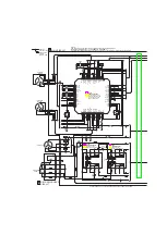
Adjustment method
Maintenance of laser pickup
Replacement of laser pickup
Description of major ICs
Attention when parts
are exchanged
1-2
1-3
1-4
1-9
1-10
1-10
1-11
1-24