background image

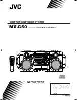
SERVICE MANUAL

COMPACT COMPONENT SYSTEM

No.20913

Feb. 2001

COPYRIGHT      2001 VICTOR COMPANY OF JAPAN, LTD.

MX-G50 / MX-G56

MX-G50/MX-G56

Area Suffix            

Area Suffix            

J
C

C

U.S.A.

Canada

Canada

Contents

Safety Precautions
Important for laser products
Preventing static electricity
Disassembly method  
Wiring connection
Adjustment method

Flow of functional operation 
                        until TOC read
Maintenance of laser pickup
Replacement of laser pickup
Trouble shooting
Description of major ICs

1-2
1-3
1-4
1-5
1-20
1-21

1-25
1-26
1-26
1-27
1-30

MX-G50

MX-G56

CA-MXG50

CA-MXG50

CA-MXG56

SP-MXG50

SP-MXG50

SP-MXG56

MX-G50 J

MX-G50 C

MX-G56 C

Each difference points

CD/DECK/

RECEIVER

Speaker

Optical

out

Color

POWER / SUB / CD EJECT /
DISK CHANGER button

SILVER

SILVER

METALLIC LIGHT GRAY

VOLUME RING

ornament

CD fitting

MODEL

SP-MXG50

SP-MXG50

CA-MXG50

CANCEL

/DEMO

PRESET

COMPU PLAY CONTROL

PLAY & EXCHANGE

STANDBY/ON

STANDBY

DISC CHANGE

SOUND

MODE

SUBWOOFER

LEVEL

CD-R

/RW  PLAYBACK

COMPACT

DIGITAL AUDIO

COMPACT COMPONENT SYSTEM

MX-G50

CLOCK
/ TIMER

DISPLAY

PHONES

REPEAT

PROGRAM

REC START

/STOP

CD
REC START

DUBBING

TAPE A

TUNING

SET

TAPE B

RANDOM

EJECT

PLAY

FULL - LOGIC CONTROL

A

EJECT

REC/PLAY

CD SYNCHRO RECORDING

B

DISC SKIP

VOLUME

VOLUME

+

Ð

RMÐSMXG50A REMOTE CONTROL

STANDBY/ON

1

2

3

4

5

6

7

8

9

10

+10

SLEEP

SUBWOOFER

LEVEL

SOUND

MODE

FM MODE

TAPE A/B

FADE 

MUTING

FM/AM

AUX

/

CD 

TAPE 

Summary of Contents for CA-MXG50

Page 1: ...G50 SP MXG56 MX G50 J MX G50 C MX G56 C Each difference points CD DECK RECEIVER Speaker Optical out Color POWER SUB CD EJECT DISK CHANGER button SILVER SILVER METALLIC LIGHT GRAY VOLUME RING ornament CD fitting MODEL SP MXG50 SP MXG50 CA MXG50 CANCEL DEMO PRESET COMPU PLAY CONTROL PLAY EXCHANGE STANDBY ON STANDBY DISC CHANGE SOUND MODE SUBWOOFER LEVEL CD R RW PLAYBACK COMPACT DIGITAL AUDIO COMPACT...

Page 2: ...e currnet check Electrical shock hazard testing After re assembling the product always perform an isolation check on the exposed metal parts of the product antenna terminals knobs metal cabinet screw heads headphone jack control shafts etc to be sure the product is safe to operate without danger of electrical shock Do not use a line isolation transformer during this check Plug the AC line cord dir...

Page 3: ... laser is able to function 6 CAUTION Use of controls adjustments or performance of procedures other than those specified herein may result in hazardous radiation exposure VARNING Osynlig laserstrålning är denna del är öppnad och spårren är urkopplad Betrakta ej strålen VARO Avattaessa ja suojalukitus ohitettaessa olet alttiina näkymättömälle lasersäteilylle Älä katso säteeseen ADVARSEL Usynlig las...

Page 4: ...up The tester s internal power source can easily destroy the laser diode 4 Handling the traverse unit optical pickup 1 Do not subject the traverse unit optical pickup to strong shocks as it is a sensitive complex unit 2 Cut off the shorted part of the flexible cable using nippers etc after replacing the optical pickup For specific details refer to the replacement procedure in the text Remove the a...

Page 5: ...n both sides of the body Remove the metal cover from the body by lifting the rear part of the cover 1 2 3 Disassembly method Main body Removing the metal cover See Fig 1 to 3 Do not break the front panel tab fitted to the metal cover ATTENTION Fig 1 Fig 2 Fig 3 Metal cover A A A Metal cover B Metal cover B B B Optical out only MX G50 J MX G56 C ...

Page 6: ...e Fig 4 to 6 Turn the black loading pulley gear marked b from the back of the CD changer unit as shown in Fig 7 and draw the CD tray toward the front After drawing the lower part of the tray fitting toward the front remove the five claws a Then while moving the tray fitting upward remove it Push and insert the CD tray manually 1 2 3 Removing the CD Tray fitting 2 See Fig 5 to 7 How to eject the CD...

Page 7: ...nner side of the main board in the body Remove the two screws C attaching the CD changer unit on the back of the body Remove the two screws D attaching the CD changer unit on the both side of the body Draw the CD changer unit upward from behind while pulling the rear panel outward 1 2 3 4 5 6 Removing the CD changer unit See Fig 8 to 10 Fig 8 Fig 9 Fig 10 a Fig 10 b CW105 CD servo board CD changer...

Page 8: ...ing the earth terminal extending from the cassette mechanism assembly Remove the screw G attaching the front panel assembly and main board Remove the screw H attaching the front panel assembly on the bottom of the body Release the two joints c on both sides and two joints d on the bottom of the body using a screwdriver 1 2 3 4 5 6 Removing the front panel assembly See Fig 11 to 13 Fig 11 Fig 12 Fi...

Page 9: ... Then pull out the heat sink AMP board inward 1 2 3 4 5 Removing the heat sink AMP board See Fig 14 and 15 Prior to performing the following procedure remove the metal cover and CD changer unit Disconnect the card wire from connector CON01 on the tuner board Remove the two screws L attaching the tuner pack 1 2 Removing the tuner pack See Fig 15 and 16 Prior to performing the following procedure re...

Page 10: ...rmer board Remove the screw G attaching the main board holder See Fig 12 Remove the two screws N attaching the heat sink and bottom chassis 1 2 3 4 Removing the main Board See Fig 18 Prior to performing the following procedure remove the metal cover heat sink AMP board tuner pack and rear cover Disconnect the power cord from connector RCW2 of the power transformer board Disconnect the harness from...

Page 11: ...wing procedure remove the FL display system control board Pull out the volume knob subwoofer knob and sound mode nob from front side Remove the ten screws V attaching the front board and release the two tabs f out ward 1 2 Removing the front board See Fig 24 Front panel assembly Prior to performing the following procedure remove the FLdisplay system control board You can pull out the headphone boa...

Page 12: ...3 Align the gear cam with the gear tray as shown fig 27 then mount the CD tray When assembling the CD tray take extreme care not engage with gear synchro 1 2 Prior to performing the following procedure remove the CD changer unit Removing the CD tray See Fig 25 to 27 Reinstall the CD tray See Fig 28 to 29 CD changer unit Fig 26 Fig 25 Fig 27 Fig 28 Fig 29 Loading pulley gear CD tray CD tray CD tray...

Page 13: ... and release the harness from the two hooks i Remove the sensor board Remove the screw Y attaching the turn table Detach the turn table from the tray Pull outward the tab marked j attaching the turn table motor assembly on the upper side of the tray and detach the turn table motor assembly from the tray 1 2 3 4 Removing the sensor board the turn table motor assembly See Fig 30 to 32 Fig 31 Fig 29 ...

Page 14: ... the screw Z attaching the switch board and release the two tabs k attaching the switch board outward and detach the switch board Remove the two screws A attaching the CD servo board and First release the n side of the two tabs l and two tabs m attaching the CD servo board motor to raise the CD servo board slightly then release the CD servo board If the tabs l and m are hard to release it is recom...

Page 15: ...the CD mechanism holder assembly Pull outward the stopper fixing the shaft on the left side and remove the CD mechanism holder assembly from behind in the direction of the arrow y Turn the CD mechanism holder assembly half around the lift up slide shaft n of the CD mechanism holder assembly until the turn table is reversed and pull out the CD mechanism holder assembly 1 2 3 Removing the CD mechani...

Page 16: ...ws A fixing the pickup shaft 3 Removing the pickup unit Removing the feed motor See Fig 1 Remove the two motor fixing screws at B and removing the feed motor Removing the spindle motor The spindle motor cannot be removed as a single unit When removing the spindle motor change the chasis and turntable together as aunit A A B Shaft Feed Gear Shutter Pickup unit Motor board Unsolder Feed motor Spindl...

Page 17: ... erase head Remove the screw C fixing the erase head Fig 1 Removing the pinch roller 1 Pull out the pinch roller by opening the pinch roller stopper outward to unlock Fig 3 2 When reassembling the pinch roller refer to fig 4 to hook up the spring Fig 1 Fig 2 Fig 3 Fig 4 R P Head R P Head E Head Spring Stoppsr Pinch roller assembly A A B B C Pinch roller Pinch roller stopper Pinch roller Pinch roll...

Page 18: ...grease s splash when the drive belt comes off Fig 5 Fig 6 2 Unsolder the motor terminal Fig 5 Removing the mechanism board 1 Unsolder the four parts a on the solenoid coil terminal Fig 5 2 Remove the two screws E fixing the board Fig 5 3 Unhook the three parts b from the board Fig 5 4 Remove the mechanism board Fig 5 Removing the flywheel Remove the cut washers at c and d from the capstan shaft th...

Page 19: ...move the side panel 1 Removing the side panel See Fig 1 Remove the fore screws C attaching the side speaker Pull out the side speaker and remove the speaker cord from the speaker terminal 1 2 Removing the side speaker See Fig 2 and 3 Speaker section Side panel Side speaker Front panel Side speaker Speaker terminal Fig 1 A B B C C Fig 2 Fig 3 ...

Page 20: ...mechanism RCW2 RFS2 Power transformer RFS5 RFS6 RFS7 RFS8 PCW1 ACW1 ACW2 FL display system control board 3708 000122 3708 000258 3809 001228 AH39 20002D AH39 00022A AH39 00247A AH39 00096D AH39 20025S 3809 001185 AH39 00254A AH39 00254A 3809 001224 AH39 20561P 3809 001121 16634 502 610 3809 001034 Amp board Power CD switch board Front key switch board Tuner board Main board H phone J board Color c...

Page 21: ...1 7 0 0 5V Received FREQ Adjustment point 522 1611 KHz MO AM MW RF Adjustment ITEAM 594 KHz MA Maximum Output Fig1 4 TESTER MAIN PCB VT GND Fig 1 4 OSC Voltage LW OSC Adjustment 146 290 KHz LO 2 7 0 0 5V AM MW RF Adjustment 150 KHz LA Maximum Output Fig1 4 Adjustment method 1 Tuner ...

Page 22: ...S G level to 28dB Figure1 1 IF CENTER and THD Adjustment SSG FREQ Adjustment point SVR1 98 MHz BEACON SENSITIVITY SEMI VR 20K FM S S G GND 28 dB FM S S G Output GND Speaker Terminal FM Antenna Terminal Distortion Meter Input SET Input output Oscilloscope FM IN FM Antenna SET 20 k OUTPUT AM SSG 450KHZ INPUT AM ANT IN Speaker Terminal 60cm AM IF VTVM Oscilloscope AM MW I F Adjustment Maximum output ...

Page 23: ...o the frequency counter Turn VSR1 to left and right FRONT PCB 3KHz Remark Standard To Adjust Pre Setup Item Step Pre Setup Condition 1 Deck 1 VT 712 2 Press PLAY SW button 3 Deck 2 Same as above Cassette Deck output SPK OUT Frequency Counter Figure 1 5 Figure 1 6 SPK OUT Recording Play head AZIMUTH control screw Figure 1 7 In Out Cassette Deck Oscilloscope 2 Cassette Deck range Figure 1 8 Audio OS...

Page 24: ...p Pre Setup Condition After putting MTT 114N into Deck 1 Press FWD PLAY button AZIMUTH 1 2 SPK OUT VTVM is connected to the scope T urn the control screw to as shown in Figure 1 6 Max output and same phase both channels After adjustment secure it with REGION LOCK 7mV mV Turn JSR2L JSR2R to the right and left Remark Standard To Adjust Pre Setup Item Step Pre Setup Condition Fig1 8 After putting VT ...

Page 25: ...Approx 3 7sec Pin 34 of KB9226 IC101 Approx 0 4V 2 50V Tracking error waveform at TOC reading Power ON Play Key Confirm that the voltage at the pin37 of KB9226 IC101 is 3 5V Confirm that the signal from pin24 of KB9226 IC101 is 3 5V as a accelerated pulse during approx 1 96s Confirm the waveform of the Tracking error signal at the pin 34 of KB9226 IC101 TOC reading Play a disc Confirm the eye patt...

Page 26: ...life of the laser diode has expired the following symptoms will appear 1 The level of RF output EFM output ampli tude of eye pattern will below Is the level of RFOUT under 1 1V 0 2Vp p Replace it NO YES O K 3 Semi fixed resistor on the APC PC board The semi fixed resistor on the APC printed circuit board which is attached to the pickup is used to adjust the laser power Since this adjustment should...

Page 27: ...heck the B B power source RBD1 RBD2 RW2 Check the power PCB Fuse P T RFS2 RFS5 RFS6 RFS7 RFS8 Front PCB Does UX1 6MHz oscillate Check the main PCB RIC1 L4959 Check the AMP PCB AIC1 AIC2 Check headphone jack soldering condition Check the front PCB UIC com UIC2 M66010gp Check the AMP PCB AQ2L 2R AQ1 2 3 4 Remove it with remocon Is mute selected Headphone jack short No No No No No No No No No No Yes ...

Page 28: ...MX G50 MX G56 1 28 2 Tuner malfunction FM AM 3 Tape malfunction ...

Page 29: ...MX G50 MX G56 1 29 4 CD ...

Page 30: ...VS OUT 8 6V EN 8 6V EN 12V a GND EN 12V b N C OUT 5 6V VS OUT 12V b TAB CONNECTED TO PIN 6 D97AU716A Pin Pins Description 1 OUT 12V b 12V 1 3A SWITCHED OUTPUT VOLTAGE 2 VS Supply Voltage 3 OUT 5 6V 5 6V 250mA OUTPUT VOLTAGE 4 N C not connected 5 EN 12V b Enable 12V 1 3A SWITCHED OUTPUT VOLTAGE 6 GND Ground 7 EN 12V a Enable 12V 0 8A SWITCHED OUTPUT VOLTAGE 8 EN 8 6V Enable 8 6V 0 6A SWITCHED OUTPU...

Page 31: ...1 17 10 2 3 4 5 7 6 PRE 100k B IN A AN MUTE MUTE REC PB NF 2 PB IN 2 R P SW SW IN 2 ALC OUT 2 PB OUT 2 Vcc Vcc REC GND PB OUT 1 INPUT REC BIAS RECORE I REF PLAYBACK I REF PB BIAS INPUT PRE 100k N F R P SW ALC TIME CONSTANT 100k NF PRE INPUT REC NF 2 REC IN 2 REC IN 1 REC NF 1 ALC DET PRE INPUT N F 100k MODE CONTROL BIAS CIRCUIT A B SELECT SW B IN A AN PB NF 1 PB IN 1 A B SW PB MUTE REC GND IN 1 OU...

Page 32: ...KO LCHOUT RCHOUT VHALF VREF 1 bit DAC Digital Out Digital Filter C2PO DATX SADTI LRCKI BCKI S5L9290X DSP DAC 48 LQFP 0707 VSSA_PLL VCO1LF VSSD_PLL VDDD_PLL XIN XOUT EFMI LOCK SMEF C2PO JITB DATX VDDD3 5V VDDD2 3V SBCK SQDT SMON TESTV SMDS WDCK MUTE BCKI 1 2 3 4 5 6 7 8 9 10 11 12 36 35 34 33 32 31 30 29 28 27 26 25 13 14 15 16 17 18 19 20 21 22 23 24 48 47 46 45 44 43 42 41 40 39 38 37 VDDD1_5V VS...

Page 33: ...SMEF O LPF time constant control of the spindle servo error signal 12 SMDP O Phase control output for Spindle Motor drive 13 SMDS O Speed control output for Spindle Motor drive 14 WDCK O Word clock output Normal Speed 88 2KHz Double Speed 176 4KHz 15 TESTV I Various Data Clock Input 16 LKFS O The Lock status output of frame sync 17 C4M O 4 2336MHz clock output 18 RESETB I System Reset at L 19 MLT ...

Page 34: ...ta output 34 SADTO O Serial audio data output 48 slot MSB first 35 LRCKO O Channel clock output 36 BCKO O Bit clock output 37 BCKI I Bit clock input 38 LRCKI I Channel clock input 39 SADTI I Serial audio data input 48 slot MSB first 40 VSSD_DAC Digital Ground for DAC 41 VDDD_DAC Digital Power for DAC 3V Power 42 RCHOUT O Right Channel audio output through DAC 43 VSSA_DAC Analog Ground for DAC 44 V...

Page 35: ...9 D18 D17 D1 D2 D3 D4 D5 D6 D7 D8 D9 D10 D11 D12 D13 D14 D15 D16 D1 D2 D3 D4 D5 D6 D7 D8 D9 D10 D11 D12 D13 D14 D15 D16 1 2 3 4 5 6 7 8 9 10 16 32 31 30 CLOCK INPUT CLK SET INPUT S CHIP SELECT CS INPUT SERIAL DATA DI INPUT GND GND Vcc DO SERIAL DATA OUTPUT PARALLEL DATA I O D1 D2 D3 D22 D23 D24 Control circuit Shift register 1 DO D24 D23 D22 D3 D2 D1 Q24 Q23 Q22 Q3 Q2 Q1 D24 D23 D22 D3 D2 D1 Q24 Q...

Page 36: ...tion Focus Search Offset Adjust FZC Gen EQO PD LD LPFT TEIO TZC SSTOP ATSC TEO TEM SLP SLO SLM FEO FEM SPDLO SPDLM EQI RFO RFM EQC VREF PDE PDF PDBD PDAC ISTAT MCK MDATA MLT RESET WDCK CLVI LOCK ASY EFM 5 45 46 44 43 6 7 8 9 10 11 14 13 15 16 17 19 18 20 22 21 24 23 30 29 25 26 27 28 29 36 33 34 35 37 38 39 41 40 42 47 48 1 2 3 EFMI DCCI DCC0 MCP DCB VCC VDD FRSH FSET FLB FGD FSI TGU S1L9226X TEO ...

Page 37: ...onent to change the high frequency of tracking Loop 13 ISTAT O Internal status output 14 MCK I Micom clock 15 MDATA I Data input 16 MLT I Data latch input 17 RESET I Reset input 18 CLVI I Input the spindle control output from DSP 19 WDCK I 88 2KHz input terminal from DSP 20 LOCK I Sled run away inhibit pin L sled off tracking gain up 21 EFM O EFM output for RFO slice to DSP 22 ASY I Auto asymmetry...

Page 38: ...t 40 PDBD I Photo diode B D RF I V amp inverting input 41 PDF I Photo diode F tracking F I V amp inverting input 42 PDE I Photo diode E tracking E I V amp inverting input 43 DCB I Capacitor connection to limit the defect detection 44 MCP I Capacitor connection to mirror hold 45 DCCI O Output pin to connect the component for defect detect 46 DCCO I Input pin to connect the component for defect dete...

Page 39: ... 13 14 GND GND 10K REGULATOR 10K 10K VCC VCC 10K 10K T S D 10K 10K 10K 50K MUTE LEVEL SHIFT LEVEL SHIFT STK402 090 AIC2 STK402 040 AIC1 1 Pin layout 1 2 3 4 5 6 7 8 9 10 11 12 13 14 15 ch 1 ch 2 _ _ CH1 IN CH1 NF NC Pre Vcc BIAS CH1 VE CH1 VE Vcc Vcc CH2 VE CH2 VE Pre Vco SUB GND CH2 NF CH2 IN STK402 090 STK402 090 1 15 ...

Page 40: ...SB0 P12 S CK0 P13 S O1 P14 S I1 SB1 P15 S CK1 S19 P C3 S18 P C2 S17 P C1 S16 P C0 VDD3 S15 T15 S14 T14 S13 T13 S12 T12 S11 T11 S10 T10 S9 T9 S8 T8 S7 T7 S6 T6 S5 T5 S4 T4 S3 T3 S2 T2 S1 T1 S47 P F7 S46 P F6 S45 P F5 S44 P F4 S43 P F3 S42 P F2 S41 P F1 S40 P F0 VDD4 S39 P E7 S38 P E6 S37 P E5 S36 P E4 S35 P E3 S34 P E2 S33 P E1 S32 P E0 S31 P D7 S30 P D6 S29 P D5 S28 P D4 S27 P D3 S26 P D2 S25 P D1...

Page 41: ...Generator CF RC X tal BaseTimer SIO0 SIO1 Timer0 Timer1 ADC INT0 3 NoiseFilter SIO Automatic transmission RAM 128 bytes VFD Controller HighvoltageOutput Bus Interface Port 1 Port 3 Port 7 Port 8 IR PLA PROM Control PROM 48KB PC ACC B Register C Register ALU PSW RAR RAM StackPoi nter Port 0 WatchdogTimer ...

Page 42: ...MX G50 MX G56 1 42 LA1837 IC01 FM IF DET AM RF IF DET ...

Page 43: ...6 TREBLE R 5 6nF TREBLE L 100nF 5 6K 100nF BOUT L 100nF 100nF 5 6K BIN R BOUT R 79dB CONTROL 79dB CONTROL 15 13 19 18 50K 0 47 F 50K 0 47 F 50K 0 47 F 50K 0 47 F 50K 0 47 F 50K 0 47 F 50K 31 5dB control R IN3 R IN2 R IN1 31 5dB control L IN2 L IN3 L IN4 5 6 7 3 2 1 Vref OFF SURR OFF SURR RB FIX FIX VAR RB FIX VAR L R 30K 30K 9 8 2 2 F 11 10 2 2 F MUXOUT R IN R MUXOUT L IN L L_IN3 L_IN4 MUXOUTL IN ...

Page 44: ...ed in Japan 200102 V VICTOR COMPANY OF JAPAN LIMITED AUDIO COMMUNICATION BUSINESS DIVISION PERSONAL MOBILE NETWORK BUSINESS UNIT 10 1 1chome Ohwatari machi Maebashi city 371 8543 Japan No 20913 MX G50 MX G56 ...

Page 45: ...2 1 MX G50 MX G56 A B C D E F G 1 2 3 4 5 Block diagram Only U version ...

Page 46: ... schematic diagrams TUNER signal TAPE REC signal TAPE P B signal CD signal Parts are safety assurance parts When replacing those parts make sure to use the specified one SHEET 4 5 SHEET 5 5 SHEET 3 5 SHEET 1 5 SHEET 2 5 SHEET 2 5 Main section ONLY MX G50 J MX G56 C ...

Page 47: ...2 3 MX G50 MX G56 A B C D E F G 1 2 3 4 5 Amplifier section MAIN Signal SHEET 1 5 SHEET 1 5 SHEET 2 5 Parts are safety assurance parts When replacing those parts make sure to use the specified one ...

Page 48: ...2 4 MX G50 MX G56 H A B C D E F G 1 2 3 4 5 Front control section SHEET 4 5 SHEET 3 5 SHEET 1 5 ...

Page 49: ...2 5 MX G50 MX G56 A B C D E F G 1 2 3 4 5 CD signal CD section SHEET 4 5 SHEET 1 5 SHEET 1 5 ...

Page 50: ...2 6 MX G50 MX G56 H A B C D E F G 1 2 3 4 5 Tuner section FM TUNER SIGNAL AM SIGNAL SHEET 5 5 SHEET 1 5 ...

Page 51: ...2 7 MX G50 MX G56 A B C D E F G 1 2 3 4 5 Main board Printed circuit boards ...

Page 52: ...2 8 MX G50 MX G56 H A B C D E F G 1 2 3 4 5 AMP board ...

Page 53: ...2 9 MX G50 MX G56 A B C D E F G 1 2 3 4 5 Front board Power CD switch board FL display system control board Front key switch board ...

Page 54: ...2 10 MX G50 MX G56 H A B C D E F G 1 2 3 4 5 CD Servo control board ...

Page 55: ...2 11 MX G50 MX G56 A B C D E F G 1 2 3 4 5 Tuner board Reverse side Tuner board Front side Head phone board Power transformer board ...

Reviews: