Intel XScale Core, Developer'S Manual
The Intel XScale Core Developer's Manual is an essential resource for maximizing the potential of this cutting-edge product. Detailed instructions and technical insights are provided in this comprehensive manual. Download it for free from our website and unlock the full potential of your Intel XScale Core.
Share
Download


Reviews:
No comments
Related manuals for XScale Core
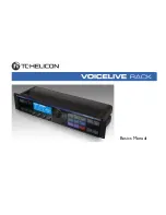
voicelive rack
Brand: TC-Helicon Pages: 18

01A99-0200
Brand: VALMETAL Pages: 38

PFP720
Brand: Prima Pages: 7

USK MCH 33526
Brand: Kalorik Pages: 28

FT-01B
Brand: Hitachi Pages: 4

HAS-K252
Brand: Hitachi Pages: 22

FL-501
Brand: Hitachi Pages: 2

POA-MD03VD2A
Brand: Sanyo Pages: 2

POA-MD17SDID
Brand: Sanyo Pages: 4

POA-FBOX130
Brand: Sanyo Pages: 3

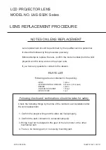
PLC-LNS07
Brand: Sanyo Pages: 3

PLC
Brand: Sanyo Pages: 3
LNS-S02K Series
Brand: Sanyo Pages: 3

LNS-W50
Brand: Sanyo Pages: 4

LNS-S30 - Zoom Lens - 48.4 mm
Brand: Sanyo Pages: 4

LNS-S30
Brand: Sanyo Pages: 4

LNS-W04
Brand: Sanyo Pages: 6

LNS-T03 - Telephoto Zoom Lens
Brand: Sanyo Pages: 8


