


NANO-PV-D4252/N4552/D5252 EPIC SBC
Page i
IEI Technology Corp.
User Manual
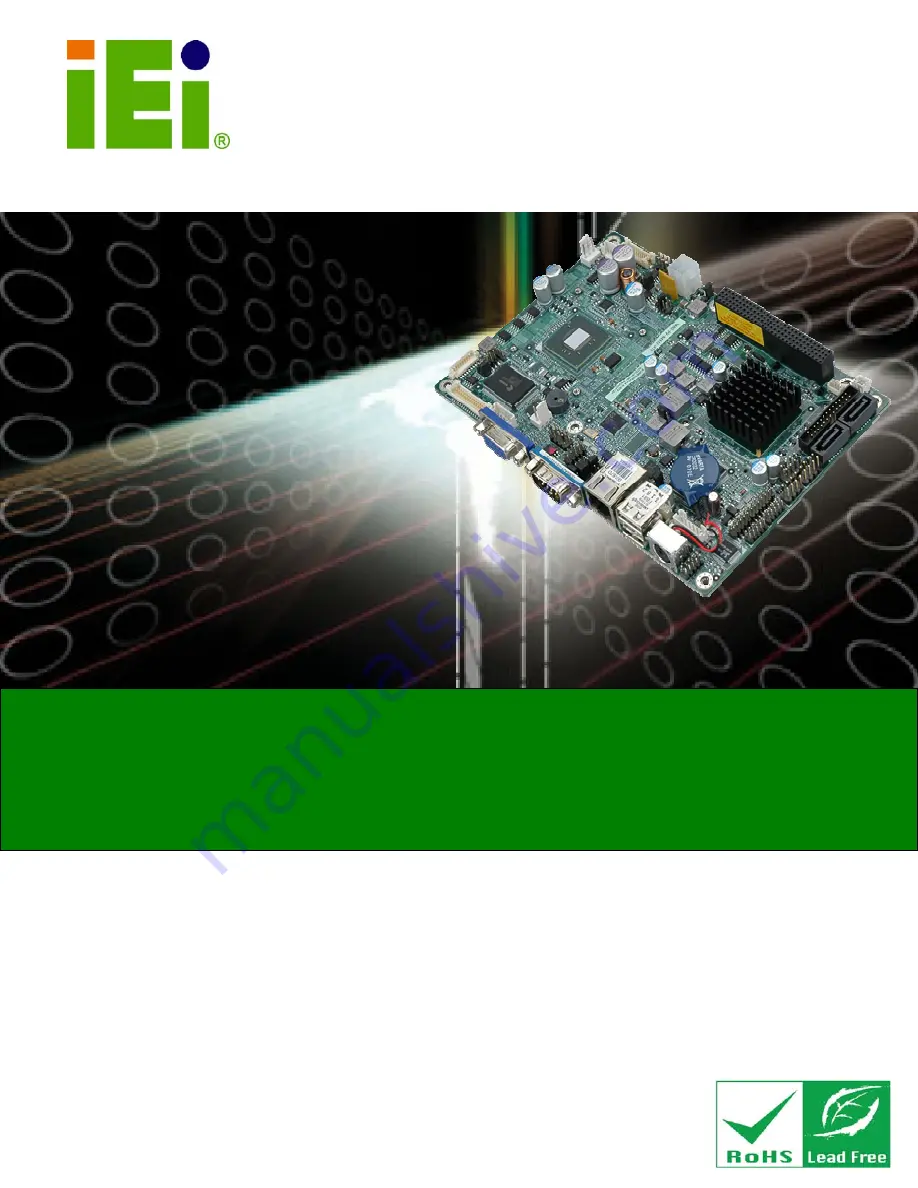
NANO-PV-D4252/N4552/D5252
MODEL:
EPIC Motherboard with Intel® Atom™ processor
D425/N455/D525, VGA, Dual LVDS, GbE LAN, Eight USB 2.0,
Two SATA 3Gb/s, Four RS-232, RS-232/422/485, PCIe mini,
PCI-104, RoHS
Rev. 1.05 – 31 December, 2011
Summary of Contents for NANO-PV-D4252
Page 14: ...NANO PV D4252 N4552 D5252 EPIC SBC Page xiv ...
Page 15: ...NANO PV D4252 N4552 D5252 EPIC SBC Page 1 Chapter 1 1 Introduction ...
Page 22: ...NANO PV D4252 N4552 D5252 EPIC SBC Page 8 2 Unpacking Chapter 2 ...
Page 26: ...NANO PV D4252 N4552 D5252 EPIC SBC Page 12 3 Connectors Chapter 3 ...
Page 54: ...NANO PV D4252 N4552 D5252 EPIC SBC Page 40 4 Installation Chapter 4 ...
Page 83: ...NANO PV D4252 N4552 D5252 EPIC SBC Page 69 5 BIOS Screens Chapter 5 ...
Page 115: ...NANO PV D4252 N4552 D5252 EPIC SBC Page 101 Appendix B B One Key Recovery ...
Page 121: ...NANO PV D4252 N4552 D5252 EPIC SBC Page 107 Figure B 3 Partition Creation Commands ...
Page 138: ...NANO PV D4252 N4552 D5252 EPIC SBC Page 124 Appendix C C Terminology ...
Page 142: ...NANO PV D4252 N4552 D5252 EPIC SBC Page 128 Appendix D D Watchdog Timer ...
Page 145: ...NANO PV D4252 N4552 D5252 EPIC SBC Page 131 Appendix E E Hazardous Materials Disclosure ...


