background image

Page 1 


RF65 


Tel: +86-755-82973805    Fax: +86-755-82973550    E-mail: [email protected] http://www.hoperf.com


Part Number


Delivery


MOQ / Multiple


RF65


Tape & Reel


3000 pieces


D

ec

im

a

ti

o

n

 a

n

d


&

 F

il

te

ri

ng


D

e

m

o

d

u

lat

or

 & 

B

it


S

y

n

c

h

ro

n

iz

e

P

a

c

k

e

E

n

g

in

e

 &

 66

 By

te

s


F

IFO


C

o

n

tr

ol

 R

e

g

is

te

rs

 -

 Sh

if

 R

eg

is

te

rs

 -

 SPI


In

te

rf

a

c

e


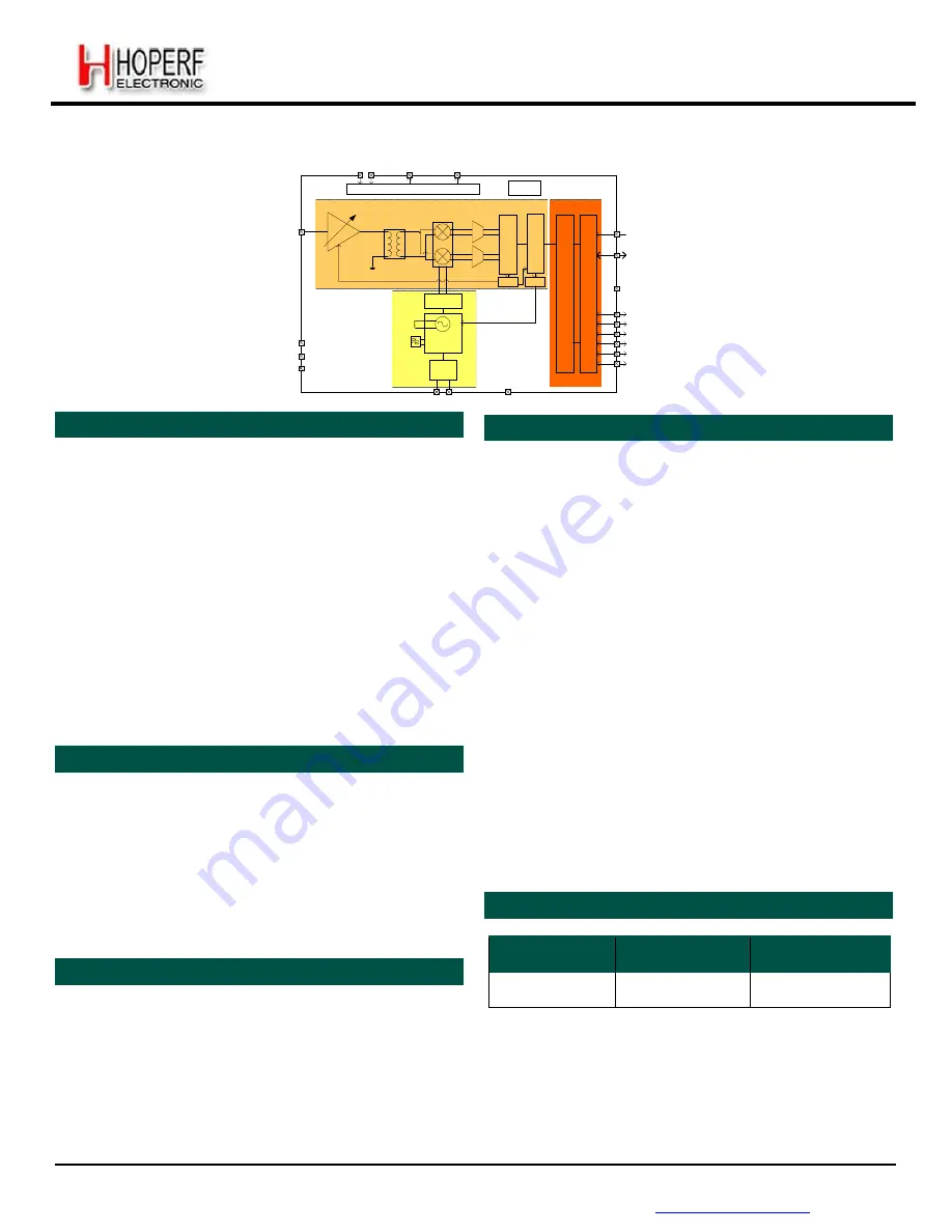
Low Power Integrated UHF Receiver With -120dBm High Sensitivity


VBAT1&2  

VR_ANA  

VR_DIG 


Power  Distribution System 


RC 

Oscillator 


RFIN 


LNA 


Single  to 

Differential 


Mixers 

Σ/Δ 

Modulators 


RESET 


SPI 


Division by 

2,  4 or  6 

RSSI  

AFC 


GND 


Tank 

Inductor 


Loop 

NC 

Filter 

NC 

NC 


Frac-N PLL 
Synthesizer 


XO 

32  MHz 

DIO0 

DIO1 

DIO2 

DIO3 

DIO4 

DIO5 


GENERAL DESCRIPTION


XTAL 

GND 


KEY PRODUCT FEATURES


The  RF65  is  a  highly  integrated RF  receiver  capable  of 
operation  over  a  wide  frequency range,  including the 
3 1 5 , 433,868 and 915 MHz license-free ISM (Industry 
Scientific and Medical) frequency bands. Its highly 
integrated architecture allows for a minimum of external 
components whilst maintaining maximum design flexibility. 
All major RF communication parameters are programmable 
and most of them can be dynamically set. The RF65 offers 
the unique advantage of programmable narrow-band and 
wide-band communication modes without the need to 
modify external components. The RF65 is optimized for 
low power consumption while offering high sensitivity and 
channelized operation. TrueRF

™ technology enables a 

lowcost external component count  (elimination of  the  SAW 
filter)  whilst  still satisfying ETSI and FCC regulations. 


APPLICATIONS


Automated Meter Reading 


Wireless Sensor Networks 


Home and Building Automation 


Wireless Alarm and Security Systems 


Industrial Monitoring and Control 


High Sensitivity: down to -120 dBm at 1.2 kbps 


High Selectivity: 16-tap FIR Channel Filter 


Bullet-proof front end: IIP3 = -18 dBm, IIP2 = +35 dBm, 

80 dB Blocking Immunity, no Image Frequency response 


Low current: Rx = 16 mA, 100nA register retention 


Constant RF performance over voltage range of chip 


FSK Bit rates up to 300 kb/s 


Fully integrated synthesizer with a resolution of 61 Hz 


FSK, GFSK, MSK, GMSK and OOK demodulation 


Built-in Bit Synchronizer performing Clock Recovery 


Incoming Sync Word Recognition 


115 dB+ Dynamic Range RSSI 


Automatic RF Sense with ultra-fast AFC 


Packet engine with CRC, AES-128 encryption and 66- 

byte FIFO 


Built-in temperature sensor and Low Battery indicator 


ORDERING INFORMATION


MARKETS


Europe: EN 300-220-1 


North America: FCC Part 15.247, 15.249, 

15.231 


Narrow Korean and Japanese bands 


QFN 28 Package - Operating Range [-40;+85°C] 


Pb-free, Halogen free, RoHS/WEEE compliant product 

Summary of Contents for RF 65

Page 1: ...ommunication modes without the need to modify external components The RF65 is optimized for low power consumption while offering high sensitivity and channelized operation TrueRF technology enables a lowcost external component count elimination of the SAW filter whilst still satisfying ETSI and FCC regulations APPLICATIONS Automated Meter Reading Wireless Sensor Networks Home and Building Automati...

Page 2: ...ower Consumption 12 2 4 2 Frequency Synthesis 12 2 4 3 Receiver 13 2 4 4 Digital Specification 14 3 Chip Description 15 3 1 Power Supply Strategy 15 3 2 Low Battery Detector 15 3 3 Frequency Synthesis 15 3 3 1 Reference Oscillator 15 3 3 2 CLKOUT Output 16 3 3 3 PLL Architecture 16 3 3 4 Lock Time 17 3 3 5 Lock Detect Indicator 17 3 4 Receiver Description 17 3 4 1 Block Diagram 17 3 4 2 LNA Single...

Page 3: ...perature Sensor 29 3 4 19 Timeout Function 29 4 Operating Modes 30 4 1 Basic Modes 30 4 2 Automatic Sequencer and Wake Up Times 30 4 2 1 Receiver Startup Time 30 4 2 2 Rx Start Procedure 32 4 2 3 Optimized Frequency Hopping Sequences 32 4 3 Listen Mode 33 4 3 1 Timings 33 4 3 2 Criteria 34 4 3 3 End of Cycle Actions 34 4 3 4 RC Timer Accuracy 35 4 4 AutoModes 36 5 Data Processing 37 5 1 Overview 3...

Page 4: ...or Threshold Default Setting 71 9 4 AFC Control 71 9 4 1 AfcAutoClearOn 71 9 4 2 AfcLowBetaOn and LowBetaAfcOffset 71 9 5 ContinuousDagc 71 ADVANCED COMMUNICATIONS SENSING DATASHEET 6 4 IRQ and Pin Mapping Registers 60 6 5 Packet Engine Registers 62 6 6 Temperature Sensor Registers 65 6 7 Test Registers 65 7 Application Information 66 7 1 Crystal Resonator Specification 66 7 2 Reset of the Chip 66...

Page 5: ...quence no wanted signal is received 33 Figure 18 Listen Mode Sequence wanted signal is received 35 Figure 19 Auto Modes of Packet Handler 36 Figure 20 RF65 Data Processing Conceptual View 37 Figure 21 SPI Timing Diagram single access 38 Figure 22 FIFO and Shift Register SR 39 Figure 23 FifoLevel IRQ Source Behavior 40 Figure 24 Sync Word Recognition 41 Figure 25 Continuous Mode Conceptual View 43 ...

Page 6: ...mmary 19 Table 10 Available RxBw Settings 21 Table 11 Bit Rate Examples 23 Table 12 Basic Receiver Modes 30 Table 13 Range of Durations in Listen Mode 33 Table 14 Signal Acceptance Criteria in Listen Mode 34 Table 15 End of Listen Cycle Actions 34 Table 16 Status of FIFO when Switching Between Different Modes of the Chip 40 Table 17 DIO Mapping Continuous Mode 42 Table 18 DIO Mapping Packet Mode 4...

Page 7: ... Locked Loop FCC Federal Communications Commission POR Power On Reset Fdev Frequency Deviation RBW Resolution BandWidth FIFO First In First Out RF Radio Frequency FIR Finite Impulse Response RSSI Received Signal Strength Indicator FS Frequency Synthesizer Rx Receiver FSK Frequency Shift Keying SAW Surface Acoustic Wave GUI Graphical User Interface SPI Serial Peripheral Interface IC Integrated Circ...

Page 8: ...ant RF performance is required over the full operating range of the device down to 1 8V The RF65 is intended for applications over a wide frequency range including the 433 MHz and 868 MHz European and the 902 928 MHz North American ISM bands Coupled with a very aggressive sensitivity the advanced system features of the RF65 include a 66 byte RX FIFO configurable automatic packet handler listen mod...

Page 9: ...p www hoperf com ADVANCED COMMUNICATIONS SENSING DATASHEET 1 2 Pin and Marking Diagram The following diagram shows the pin arrangement of the QFN package top view Figure 2 Pin Diagram Notes yyww refers to the date code xxxxxx refers to the lot number Figure 3 Marking Diagram RF65 ...

Page 10: ... GND or Do not connect 8 DIO0 I O Digital I O software configured 9 DIO1 DCLK O Digital Output software configured 10 DIO2 DATA O Digital Output software configured 11 DIO3 I O Digital I O software configured 12 DIO4 I O Digital I O software configured 13 DIO5 I O Digital I O software configured 14 NC Connect to GND or Do not connect 15 VBAT2 Supply voltage 16 GND Ground 17 SCK I SPI Clock input 1...

Page 11: ...er pins It should thus be handled with all the necessary ESD precautions to avoid any permanent damage 2 2 Absolute Maximum Ratings Stresses above the values listed below may cause permanent device failure Exposure to absolute maximum ratings for extended periods may affect device reliability Table 2 Absolute Maximum Ratings Symbol Description Min Max Unit VDDmr Supply Voltage 0 5 3 9 V Tmr Temper...

Page 12: ...lator enabled 1 2 uA IDDST Supply current in standby mode Crystal oscillator enabled 1 25 1 5 mA IDDFS Supply current in synthesizer mode 9 mA IDDR Supply current in receive mode 16 mA 2 4 2 Frequency Synthesis Table 5 Frequency Synthesizer Specification Symbol Description Conditions Min Typ Max Unit FR Synthesizer Frequency Range Programmable 290 424 862 340 510 1020 MHz MHz MHz FXOSC Crystal osc...

Page 13: ...tion Offset 25 kHz Offset 50 kHz 37 42 42 dB dB BI Blocking Immunity Offset 1 MHz Offset 2 MHz Offset 10 MHz 45 40 32 dBm dBm dBm Blocking Immunity Wanted signal at sensitivity 16dB Offset 1 MHz Offset 2 MHz Offset 10 MHz 36 33 25 dBm dBm dBm AMR AM Rejection AM modulated interferer with 100 modulation depth fm 1 kHz square Offset 1 MHz Offset 2 MHz Offset 10 MHz 45 40 32 dBm dBm dBm IIP2 2nd orde...

Page 14: ...d Table 7 Digital Specification Symbol Description Conditions Min Typ Max Unit VIH Digital input level high 0 8 VDD VIL Digital input level low 0 2 VDD VOH Digital output level high Imax 1 mA 0 9 VDD VOL Digital output level low Imax 1 mA 0 1 VDD FSCK SCK frequency 10 MHz tch SCK high time 50 ns tcl SCK low time 50 ns trise SCK rise time 5 ns tfall SCK fall time 5 ns tsetup MOSI setup time from MO...

Page 15: ...hesis The LO generation on the RF65 is based on a state of the art fractional N PLL The PLL is fully integrated with automatic calibration 3 3 1 Reference Oscillator The crystal oscillator is the main timing reference of the RF65 It is used as a reference for the frequency synthesizer and as a clock for the digital processing The XO startup time TS_OSC depends on the actual XTAL being connected on...

Page 16: ...are both fully integrated removing the need for an external tight tolerance high Q inductor in the VCO tank circuit 3 3 3 1 VCO The VCO runs at 2 4 or 6 times the RF frequency respectively in the 915 434 and 315 MHz bands to reduce any LO leakage in receiver mode to improve the quadrature precision of the receiver The VCO calibration is fully automated A coarse adjustment is carried out at power o...

Page 17: ... be made available on some of the DIO pins and is toggled high when the PLL reaches its locking range Please refer to Table 17 and Table 18 to map this interrupt to the desired pins 3 4 Receiver Description The RF65 features a digital receiver with the analog to digital conversion process being performed directly following the LNA Mixers block The zero IF receiver is able to handle G FSK and G MSK...

Page 18: ...sensitivity linearity trade off Regardless of the data transfer mode Packet or Continuous the following series of events takes place when the receiver is enabled The receiver stays in WAIT mode until RssiValue exceeds RssiThreshold for two consecutive samples Its power consumption is the receiver power consumption When this condition is satisfied the receiver automatically selects the most suitabl...

Page 19: ...hresh1 Pin AgcThresh2 G2 31 13 15 40 AgcThresh2 Pin AgcThresh3 G3 26 18 8 48 AgcThresh3 Pin AgcThresh4 G4 14 27 1 62 AgcThresh4 Pin AgcThresh5 G5 6 36 13 68 AgcThresh5 Pin G6 0 44 20 75 3 4 3 1 RssiThreshold Setting For correct operation of the AGC RssiThreshold in RegRssiThresh must be set to the sensitivity of the receiver The receiver will remain in WAIT mode until RssiThreshold is exceeded Not...

Page 20: ...F signal to base band and offer both high IIP2 and IIP3 responses In the lower bands of operation 290 to 510 MHz the multi phase mixing architecture with weighted phases improves the rejection of the LO harmonics in receiver mode hence increasing the receiver immunity to out of band interferers The I and Q digitalization is made by two 5th order continuous time Sigma Delta Analog to Digital Conver...

Page 21: ... 6 01b 20 6 6 3 3 1 00b 16 6 7 8 3 9 10b 24 5 10 4 5 2 01b 20 5 12 5 6 3 00b 16 5 15 6 7 8 10b 24 4 20 8 10 4 01b 20 4 25 0 12 5 00b 16 4 31 3 15 6 10b 24 3 41 7 20 8 01b 20 3 50 0 25 0 00b 16 3 62 5 31 3 10b 24 2 83 3 41 7 01b 20 2 100 0 50 0 00b 16 2 125 0 62 5 10b 24 1 166 7 83 3 01b 20 1 200 0 100 0 00b 16 1 250 0 125 0 10b 24 0 333 3 166 7 01b 20 0 400 0 200 0 00b 16 0 500 0 250 0 3 4 7 DC Ca...

Page 22: ...mount of energy available within the receiver channel bandwidth Its resolution is 0 5 dB and it has a wide dynamic range to accommodate both small and large signal levels that may be present Its acquisition time is very short taking only 2 bit periods The RSSI sampling must occur during the reception of preamble in FSK and constant 1 reception in OOK Note The receiver is capable of automatic gain ...

Page 23: ...153846 1 Classical modem baud rates multiples of 0 9 kbps 0x02 0x2C 57 6 kbps 57553 95 0x01 0x16 115 2 kbps 115107 9 Round bit rates multiples of 12 5 25 and 50 kbps 0x0A 0x00 12 5 kbps 12 5 kbps 12500 00 0x05 0x00 25 kbps 25 kbps 25000 00 0x02 0x80 50 kbps 50000 00 0x01 0x40 100 kbps 100000 0 0x00 0xD5 150 kbps 150234 7 0x00 0xA0 200 kbps 200000 0 0x00 0x80 250 kbps 250000 0 0x00 0x6B 300 kbps 29...

Page 24: ... of the RSSI reduced by 6dB In the absence of an input signal or during the reception of a logical 0 the acquired peak value is decremented by one OokPeakThreshStep every OokPeakThreshDec period When the RSSI output is null for a long time for instance after a long string of 0 received or if no transmitter is present the peak threshold level will continue falling until it reaches the Floor Thresho...

Page 25: ...timization complete Figure 9 Floor Threshold Optimization The new floor threshold value found during this test should be used for OOK reception with those receiver settings 3 4 13 2 Optimizing OOK Demodulator for Fast Fading Signals A sudden drop in signal strength can cause the bit error rate to increase For applications where the expected signal drop can be estimated the following OOK demodulato...

Page 26: ...f 12 bits is required for synchronization from the RxReady interrupt The subsequent payload bit stream must have at least one transition form 0 to 1 or 1 to 0 every 16 bits during data transmission The bit rate matching between the transmitter and the receiver must be better than 6 5 Notes If the Bit Rates of Transmitter and Receiver are known to be the same the RF65 will be able to receive an inf...

Page 27: ...he signal can be evaluated as follows double side bandwidth The frequency error in Hz can be calculated with the following formula FEI FSTEP FeiValue RF65 in Rx mode Preamble modulated input signal Signal level Sensitivity Set FeiStart 1 FeiDone No 1 Yes Read FeiValue Figure 11 FEI Process 3 4 16 Automatic Frequency Correction The AFC is based on the FEI block and therefore the same input signal a...

Page 28: ...r to avoid desensitization This can be simply done by modifying Frf in RegFrfLsb A good rule of thumb is to offset the receiver s LO by 10 of the expected transmitter frequency deviation For narrow band systems it is recommended to perform AFC The RF65 has a dedicated AFC enabled when AfcLowBetaOn in RegAfcCtrl is set to 1 A frequency offset programmable through LowBetaAfcOffset in RegTestAfc is a...

Page 29: ...pValue t TempValue t 1 Returns 150d typ Needs calibration 40 C t t 1 Ambient 85 C Figure 13 Temperature Sensor Response It takes less than 100 microseconds for the RF65 to evaluate the temperature from setting TempMeasStart to 1 to TempMeasRunning reset 3 4 19 Timeout Function The RF65 includes a Timeout function which allows it to automatically shut down the receiver after a receive sequence and ...

Page 30: ...er mode and finally when the PLL has locked to Receive mode The crystal oscillator wake up time TS_OSC is directly related to the time for the crystal oscillator to reach its steady state It depends notably on the crystal characteristics The frequency synthesizer wake up time TS_FS is directly related to the time needed by the PLL to reach its steady state The signal PLL_LOCK provided on an extern...

Page 31: ...group delay DC Cutoff s group delay RSSI sampling Reception of Packet Tana Tcf Tdcc Trssi Trssi Tcf Tdcc Trssi ModeReady RxReady Figure 15 Rx Startup AGC no AFC Rx startup request sequencer or user TS_RE_AGC AFC The LNA gain is adjusted by the AGC according to the RSSI result Carrier Frequency is adjusted by the AFC XO Started and PLL is locked Analog FE s group delay Channel Filter s group delay ...

Page 32: ... DATA right after the RxReady interrupt In Packet mode the receiver will start locking its Bit Synchronizer on a minimum or 12 bits of received preamble see section 3 4 14 for details before the reception of correct Data or Sync Word if enabled can occur 4 2 3 Optimized Frequency Hopping Sequences In a frequency hopping like application it is required to turn off the receiver when hopping from one...

Page 33: ...Figure 17 tListenIdle Rx Idle Rx time tListenRx tListenRx Figure 17 Listen Mode Sequence no wanted signal is received 4 3 1 Timings The duration of the Idle phase is given by tListenIdle The time during which the receiver is on and waits for a signal is given by tListenRx tListenRx includes the wake up time of the receiver described in section 4 2 1 This duration can be programmed in the configura...

Page 34: ...nal Acceptance Criteria in Listen Mode ListenCriteria Input Signal Power RssiThreshold SyncAddressMatch 0 Required Not Required 1 Required Required 4 3 3 End of Cycle Actions The action taken after detection of a packet is defined by ListenEnd in RegListen3 as described in the table below Table 15 End of Listen Cycle Actions ListenEnd Description 00 Chip stays in Rx mode Listen mode stops and must...

Page 35: ... wanted signal is received Listen mode can be disabled by writing ListenOn to 0 4 3 4 RC Timer Accuracy All timings of the Listen Mode rely on the accuracy of the internal low power RC oscillator This oscillator is automatically calibrated at the device power up and it is a user transparent process For applications enduring large temperature variations and for which the power supply is never remov...

Page 36: ...pendently of each other i e both should be enabled at the same time The initial and the final state is the one configured in the Mode in RegOpMode The initial final states can be different by configuring the modes register while the chip is in intermediate mode The pictorial description of the auto modes is shown below Intermediate State defined by IntermediateMode EnterCondition ExitCondition Ini...

Page 37: ...h with their own data path through the data processing section Depending on the data operation mode selected some control blocks are active whilst others remain disabled 5 1 2 Data Operation Modes The RF65 has two different data operation modes selectable by the user Continuous mode each bit received is accessed in real time at the DIO2 DATA pin This mode may be used if adequate external signal pr...

Page 38: ...ress the FIFO The address is not automatically incremented but is memorized and does not need to be sent between each data byte The NSS pin goes low at the beginning of the frame and stay low between each byte It goes high only after the last byte transfer Figure below shows a typical SPI single access to a register Figure 21 SPI Timing Diagram single access MOSI is generated by the master on the ...

Page 39: ...is is illustrated in Figure 22 byte1 byte0 FIFO Rx Data 1 8 SR 8bits MSB LSB Figure 22 FIFO and Shift Register SR Note When switching to Sleep mode the FIFO can only be used once the ModeReady flag is set quasi immediate from all modes 5 2 2 2 Size The FIFO size is fixed to 66 bytes 5 2 2 3 Interrupt Sources and Flags FifoNotEmpty FifoNotEmpty interrupt source is low when byte 0 i e whole FIFO is ...

Page 40: ...mments Stdby Sleep Not cleared Sleep Stdby Not cleared Stdby Sleep Rx Cleared Rx Stdby Sleep Not cleared To allow the user to read FIFO in Stdby Sleep mode after Rx 5 2 3 Sync Word Recognition 5 2 3 1 Overview Sync word recognition also called Pattern recognition is activated by setting SyncOn in RegSyncConfig The bit synchronizer must also be activated in continuous mode automatically done in Pac...

Page 41: ...e that this incoming packet is for the node and can be processed accordingly SyncAddressMatch is cleared when leaving Rx or FIFO is emptied 5 2 3 2 Configuration Size Sync word size can be set from 1 to 8 bytes i e 8 to 64 bits via SyncSize in RegSyncConfig Error tolerance The number of errors tolerated in the Sync word recognition can be set from 0 to 7 bits to via SyncTol Value The Sync word val...

Page 42: ...eady Data RxReady Timeout 10 LowBat SyncAddress AutoMode Data LowBat Rssi 11 ModeReady PllLock Timeout Data SyncAddress ModeReady 5 3 2 DIO Pins Mapping in Packet Mode Table 18 DIO Mapping Packet Mode Mode Diox Mapping DIO5 DIO4 DIO3 DIO2 DIO1 DIO0 Sleep 00 FifoFull FifoNotEmpty FifoLevel 01 FifoFull 10 LowBat LowBat LowBat LowBat FifoNotEmpty LowBat 11 ModeReady AutoMode Stdby 00 ClkOut FifoFull ...

Page 43: ...Mode Conceptual View 5 4 2 Rx Processing If the bit synchronizer is disabled the raw demodulator output is made directly available on DATA pin and no DCLK signal is provided Conversely if the bit synchronizer is enabled synchronous cleaned data and clock are made available respectively on DIO2 DATA and DIO1 DCLK pins DATA is sampled on the rising edge of DCLK and updated on the falling edge as ill...

Page 44: ...ve tasks within the RF chip itself Another important feature is ability to empty the FIFO in Sleep Stdby mode ensuring optimum power consumption and adding more flexibility for the software CONTROL DIO0 DIO1 DIO2 DIO3 DIO4 DIO5 Data Rx SYNC RECOG PACKET HANDLER FIFO SR SPI NSS SCK MOSI MISO Figure 27 Packet Mode Conceptual View Note The Bit Synchronizer is automatically enabled in Packet mode 5 5 ...

Page 45: ...C 2 bytes Payload min 1 Byte Fields processed and removed in Rx Optional User provided fields which are part of the payload Message part of the payload Figure 28 Fixed Length Packet Format 5 5 2 2 Variable Length Packet Format Variable length packet format is selected when bit PacketFormat is set to 1 This mode is useful in applications where the length of the packet is not known in advance and ca...

Page 46: ...th is set to 0 The user can then receive packets of arbitrary length and PayloadLength register is not used in Rx modes for counting the length of the bytes received This mode is a replacement for the legacy buffered mode in RF63 RF64 transceivers The data processing features like Address filtering Manchester decoding and data dewhitening are not available if the sync pattern length is set to zero...

Page 47: ...heck is performed if CrcOn 1 and the result is available in CrcOk indicating that the CRC was successful An interrupt PayloadReady is also generated on DIO0 as soon as the payload is available in the FIFO The payload available in the FIFO can also be read in Sleep Standby mode If the CRC fails the PayloadReady interrupt is not generated and the FIFO is cleared This function can be overridden by se...

Page 48: ...ent FIFO overrun 1 Start reading bytes from the FIFO when FifoNotEmpty or FifoThreshold becomes set 2 Suspend reading from the FIFO if FifoNotEmpty clears before all bytes of the message have been read 3 Continue to step 1 until PayloadReady or CrcOk fires 4 Read all remaining bytes from the FIFO either in Rx or Sleep Standby mode Note AES decryption is not feasible on large packets since all Payl...

Page 49: ...ipped off the packet and is made available in the FIFO 5 5 6 3 Length Based In variable length Packet mode PayloadLength must be programmed with the maximum payload length permitted If received length byte is smaller than this maximum then the packet is accepted and processed otherwise it is discarded Please note that the received length byte as part of the payload is not stripped off the packet a...

Page 50: ...ip rate Manchester decoding is only applied to the payload and CRC checksum while preamble and Sync word are kept NRZ However the chip rate from preamble to CRC is the same and defined by BitRate in RegBitRate Chip Rate Bit Rate NRZ 2 x Bit Rate Manchester Manchester decoding is thus made transparent for the user who still retrieves NRZ data from the FIFO 1 BR Sync 1 BR Payload RF chips BR 1 1 1 0...

Page 51: ...hitening process is enabled if DcFree 10 The data including payload and 2 byte CRC checksum is de whitened by XORing it with a random sequence generated in a 9 bit LFSR shown in Figure 33 Payload de whitening is thus made transparent for the user who still retrieves NRZ data from the FIFO Received Data De whitened Data Figure 33 Data De Whitening ...

Page 52: ...ed05 0x00 0x06 Reserved06 0x52 0x07 RegFrfMsb 0xE4 RF Carrier Frequency Most Significant Bits 0x08 RegFrfMid 0xC0 RF Carrier Frequency Intermediate Bits 0x09 RegFrfLsb 0x00 RF Carrier Frequency Least Significant Bits 0x0A RegOsc1 0x41 RC Oscillators Settings 0x0B RegAfcCtrl 0x00 AFC control in low modulation index situations 0x0C RegLowBat 0x02 Low Battery Indicator Settings 0x0D RegListen1 0x92 L...

Page 53: ...ettings 0x24 RegRssiValue 0xFF RSSI value in dBm 0x25 RegDioMapping1 0x00 Mapping of pins DIO0 to DIO3 0x26 RegDioMapping2 0x05 0x07 Mapping of pins DIO4 and DIO5 ClkOut frequency 0x27 RegIrqFlags1 0x80 Status register PLL Lock state Timeout RSSI Threshold 0x28 RegIrqFlags2 0x00 Status register FIFO handling flags Low Battery detection 0x29 RegRssiThresh 0xFF 0xE4 RSSI Threshold control 0x2A RegRx...

Page 54: ...rol 0x4F RegTemp2 0x00 Temperature readout 0x58 RegTestLna 0x1B Sensitivity boost 0x6F RegTestDagc 0x00 0x30 Fading Margin Improvement 0x71 RegTestAfc 0x00 AFC offset for low modulation index AFC 0x50 RegTest Internal test registers Note Reset values are automatically refreshed in the chip at Power On Reset Default values are the HopeRF recommended register values optimizing the device operation R...

Page 55: ... Receiver s operating modes 000 sleep mode SLEEP 001 standby mode STDBY 010 frequency synthesizer mode FS 100 receiver mode RX others reserved Reads the value corresponding to the current chip mode 1 0 r 00 unused RegDataModul 0x02 7 r 0 unused 6 5 DataMode rw 00 Data processing mode 00 Packet mode 01 reserved 10 Continuous mode with bit synchronizer 11 Continuous mode without bit synchronizer 4 3...

Page 56: ... of the LowBat threshold 000 1 695 V 001 1 764 V 010 1 835 V 011 1 905 V 100 1 976 V 101 2 045 V 110 2 116 V 111 2 185 V RegListen1 0x0D 7 6 ListenResolIdle rw 10 Resolution of Listen modes timings calibrated RC osc 0101 64 us 1010 4 1 ms 1111 262 ms Others reserved 5 4 ListenResolRx rw 01 Resolution of Listen mode Rx time calibrated RC osc 00 reserved 01 64 us 10 4 1 ms 11 262 ms 3 ListenCriteria...

Page 57: ...uration of the Idle phase in Listen mode tListenIdle ListenCoefIdle ListenResolIdle RegListen3 0x0F 7 0 ListenCoefRx rw 0x20 Duration of the Rx phase in Listen mode startup time included see section 4 2 1 tListenRx ListenCoefRx ListenResolRx RegVersion 0x10 7 0 Version r 0x23 Version code of the chip Bits 7 4 give the full revision number bits 3 0 give the metal mask revision number ...

Page 58: ... either manually or by the AGC 2 0 LnaGainSelect rw 000 LNA gain setting 000 gain set by the internal AGC loop 001 G1 highest gain 010 G2 highest gain 6 dB 011 G3 highest gain 12 dB 100 G4 highest gain 24 dB 101 G5 highest gain 36 dB 110 G6 highest gain 48 dB 111 reserved RegRxBw 0x19 7 5 DccFreq rw 010 Cut off frequency of the DC offset canceller DCC 4 3 RxBwMant rw 10 Channel filter bandwidth co...

Page 59: ...i 0x1E 7 r 0 unused 6 FeiDone r 0 0 FEI is on going 1 FEI finished 5 FeiStart w 0 Triggers a FEI measurement when set Always reads 0 4 AfcDone r 1 0 AFC is on going 1 AFC has finished 3 AfcAutoclearOn rw 0 Only valid if AfcAutoOn is set 0 AFC register is not cleared before a new AFC phase 1 AFC register is cleared before a new AFC phase 2 AfcAutoOn rw 0 0 AFC is performed each time AfcStart is set...

Page 60: ... Set when the operation mode requested in Mode is ready Sleep Entering Sleep mode Standby XO is running FS PLL is locked Rx RSSI sampling starts Cleared when changing operating mode 6 RxReady r 0 Set in Rx mode after RSSI AGC and AFC Cleared when leaving Rx 5 r 0 unused 4 PllLock r 0 Set in FS and Rx when the PLL is locked Cleared when it is not 3 Rssi rwc 0 Set in Rx when the RssiValue exceeds Rs...

Page 61: ...ayload is ready i e last byte received and CRC if enabled and CrcAutoClearOff is cleared is Ok Cleared when FIFO is empty 1 CrcOk r 0 Set in Rx when the CRC of the payload is Ok Cleared when FIFO is empty 0 LowBat rwc Set when the battery voltage drops below the Low Battery threshold Cleared only when set by the user RegRssiThresh 0x29 7 0 RssiThreshold rw 0xE4 RSSI trigger level for Rssi interrup...

Page 62: ...RegSyncValue1 0x2f 7 0 SyncValue 63 56 rw 0x01 1st byte of Sync word MSB byte Used if SyncOn is set RegSyncValue2 0x30 7 0 SyncValue 55 48 rw 0x01 2nd byte of Sync word Used if SyncOn is set and SyncSize 1 2 RegSyncValue3 0x31 7 0 SyncValue 47 40 rw 0x01 3rd byte of Sync word Used if SyncOn is set and SyncSize 1 3 RegSyncValue4 0x32 7 0 SyncValue 39 32 rw 0x01 4th byte of Sync word Used if SyncOn ...

Page 63: ... variable max length in Rx RegNodeAdrs 0x39 7 0 NodeAddress rw 0x00 Node address used in address filtering RegBroadcastAdrs 0x3A 7 0 BroadcastAddress rw 0x00 Broadcast address used in address filtering RegAutoModes 0x3B 7 5 EnterCondition rw 000 Interrupt condition for entering the intermediate mode 000 None AutoModes Off 001 Rising edge of FifoNotEmpty 010 Rising edge of FifoLevel 011 Rising edge...

Page 64: ...Key1 0x3E 7 0 AesKey 127 120 w 0x00 1st byte of cipher key MSB byte RegAesKey2 0x3F 7 0 AesKey 119 112 w 0x00 2nd byte of cipher key RegAesKey3 0x40 7 0 AesKey 111 104 w 0x00 3rd byte of cipher key RegAesKey4 0x41 7 0 AesKey 103 96 w 0x00 4th byte of cipher key RegAesKey5 0x42 7 0 AesKey 95 88 w 0x00 5th byte of cipher key RegAesKey6 0x43 7 0 AesKey 87 80 w 0x00 6th byte of cipher key RegAesKey7 0...

Page 65: ...can not be used while measuring temperature 1 0 r 01 unused RegTemp2 0x4F 7 0 TempValue r Measured temperature 1 C per Lsb Needs calibration for accuracy 6 7 Test Registers Table 25 Test Registers Name Address Bits Variable Name Mode Default Value Description RegTestLna 0x58 7 0 SensitivityBoost rw 0x1B High sensitivity or normal sensitivity mode 0x1B Normal mode 0x2D High sensitivity mode RegTest...

Page 66: ...d be chosen in accordance with the target operating temperature range and the receiver bandwidth selected the loading capacitance should be applied externally and adapted to the actual Cload specification of the XTAL A minimum XTAL frequency of 28 MHz is required to cover the 863 870 MHz band 29 MHz for the 902 928 MHz band 7 2 Reset of the Chip A power on reset of the RF65 is triggered at power u...

Page 67: ...6 High Z 100 us 1 Wait for 5 ms High Z Chip is ready from this point on input Figure 35 Manual Reset Timing Diagram Note whilst pin 6 is driven high an over current consumption of up to ten milliamps can be seen on VDD 7 3 Reference Design All schematics shown in this section are full schematics listing ALL required components including decoupling capacitors Figure 36 Application Schematic Note In...

Page 68: ...e 32 Receiver BOM Designator 315 MHz 433 MHz 868 MHz 915 MHz Type C3 C4 C5 C8 100 nF X7R C6 C7 15 pF COG L1 39 nH 33 nH Wirewound air core or multilayer 1 air core or multilayer 1 C1 5 6 pF 5 6 pF COG C2 12 pF 12 pF 6 8 nH 5 6 nH Notes 1 Inductor values may change when using multilayer type components ...

Page 69: ...nformation 8 1 Package Outline Drawing The RF65 is available in a 28 lead QFN package as show in Figure 37 Figure 37 Package Outline Drawing 8 2 Thermal Impedance The thermal impedance of this package is Theta ja 23 8 C W typ calculated from a package in still air on a 4 layer FR4 PCB as per the Jedec standard ...

Page 70: ...wing sub sections 9 1 RC Oscillator Calibration On the RF65 V2a RC calibration at power up needs to be performed according to the following routine RC CALIBRATION Once at POR SetRFMode RF_STANDBY WriteRegister 0x57 0x80 WriteRegister REG_OSC1 ReadRegister REG_OSC1 0x80 while ReadRegister REG_OSC1 0x40 0x00 WriteRegister REG_OSC1 ReadRegister REG_OSC1 0x80 while ReadRegister REG_OSC1 0x40 0x00 Writ...

Page 71: ...setting bit ListenOn to 0 in RegListen 9 3 OOK Floor Threshold Default Setting The following default value modification was required on the V2a silicon Figure 41 RegTestOok Description It is not required to modify this register any more on the RF65 V2b 9 4 AFC Control The following differences are observed between silicon revisions V2a and V2b 9 4 1 AfcAutoClearOn On the RF65 V2a it is required to...

Page 72: ...ronics without notice Hope Microelectronics assumes no responsibility or liability for any use of the information contained herein Nothing in this document shall operate as an express or implied license or indemnity under the intellectual property rights of Hope Microelectronics or third parties The products described in this document are not intended for use in implantation or other direct life s...

Reviews: