background image

MAY 2002

HHEA-MANUFACTURING DIVISION

PA

No. 0160

51SWX20B

DP27

57SWX20B

DP27

65SWX20B

DP27

57TWX20B

DP27D

65TWX20B

DP27D

R/C: CLU-5722TSI

CLU-121S

N

N T

T S

S C

C

D

DP

P2

27

7    D

DP

P2

27

7D

D

C

Ch

ha

as

ss

siis

s

SERVICE MANUAL

CONTENTS

IMPORTANT SAFETY INSTRUCTIONS . . . . . . . . . . . . . . . . . . . . . . . . . . . . . . . . . . . . 2
SERVICING PRECAUTIONS  . . . . . . . . . . . . . . . . . . . . . . . . . . . . . . . . . . . . . . . . . . . . 6
TECHNICAL CAUTIONS  . . . . . . . . . . . . . . . . . . . . . . . . . . . . . . . . . . . . . . . . . . . . . . 10
SPECIFICATIONS  . . . . . . . . . . . . . . . . . . . . . . . . . . . . . . . . . . . . . . . . . . . . . . . . . . . 11
CIRCUIT PROTECTION  . . . . . . . . . . . . . . . . . . . . . . . . . . . . . . . . . . . . . . . . . . . . . . 11
CAUTIONS WHEN CONNECTING/DISCONNECTING THE HV CONNECTOR  . . . . . .12
GENERAL INFORMATION  . . . . . . . . . . . . . . . . . . . . . . . . . . . . . . . . . . . . . . . . . . . . .13
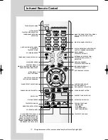
REMOTE CONTROL  . . . . . . . . . . . . . . . . . . . . . . . . . . . . . . . . . . . . . . . . . . . . . . . . .14
CUSTOMIZED PICTURE AND SOUND ADJUSTMENTS  . . . . . . . . . . . . . . . . . . . . . .15 
REAR PANEL CONNECTION  . . . . . . . . . . . . . . . . . . . . . . . . . . . . . . . . . . . . . . . . . . .19
DISPLAY PICTURE FORMATS . . . . . . . . . . . . . . . . . . . . . . . . . . . . . . . . . . . . . . . . . .25
SERVICE ADJUSTMENTS  . . . . . . . . . . . . . . . . . . . . . . . . . . . . . . . . . . . . . . . . . . . . .29
TROUBLESHOOTING  . . . . . . . . . . . . . . . . . . . . . . . . . . . . . . . . . . . . . . . . . . . . . . . .60
WAVEFORMS  . . . . . . . . . . . . . . . . . . . . . . . . . . . . . . . . . . . . . . . . . . . . . . . . . . . . . .63
DC VOLTAGE TABLES  . . . . . . . . . . . . . . . . . . . . . . . . . . . . . . . . . . . . . . . . . . . . . . . .67
PROTECTION CIRCUIT BLOCK DIAGRAM  . . . . . . . . . . . . . . . . . . . . . . . . . . . . . . . .83
CIRCUIT SCHEMATIC DIAGRAM . . . . . . . . . . . . . . . . . . . . . . . . . . . . . . . . . . . . . . . .85
PRINTED CIRCUIT BOARDS  . . . . . . . . . . . . . . . . . . . . . . . . . . . . . . . . . . . . . . . . . . .96
BLOCK DIAGRAM  . . . . . . . . . . . . . . . . . . . . . . . . . . . . . . . . . . . . . . . . . . . . . . . . . .108
WIRING DIAGRAM . . . . . . . . . . . . . . . . . . . . . . . . . . . . . . . . . . . . . . . . . . . . . . . . . .109
FINAL WIRING DRAWING  . . . . . . . . . . . . . . . . . . . . . . . . . . . . . . . . . . . . . . . . . . . .110
TROUBLESHOOTING BLOCK DIAGRAMS  . . . . . . . . . . . . . . . . . . . . . . . . . . . . . . .112
EXPLODED VIEW  . . . . . . . . . . . . . . . . . . . . . . . . . . . . . . . . . . . . . . . . . . . . . . . . . .138
EXPLODED VIEW PARTS LIST  . . . . . . . . . . . . . . . . . . . . . . . . . . . . . . . . . . . . . . . .144
REPLACEMENT PARTS LIST . . . . . . . . . . . . . . . . . . . . . . . . . . . . . . . . . . . . . . . . . .149
QUICK REFERENCE PARTS LIST  . . . . . . . . . . . . . . . . . . . . . . . . . . . . . . . . . . . . . .177
DISASSEMBLY INSTRUCTIONS  . . . . . . . . . . . . . . . . . . . . . . . . . . . . . . . . . . . . . . .178
DISASSEMBLY/ASSEMBLY INSTRUCTIONS FOR 65” SPLIT PTV . . . . . . . . . . . . . .183

CAUTION: 

These servicing instructions are for use by qualified service personnel only. To reduce the risk of

electric shock do not perform any servicing other than that contained in the operating instructions
unless you are qualified to do so. Before servicing this chassis, it is important that the service
technician read the “IMPORTANT SAFETY INSTRUCTIONS” in this service manual.

SAFETY NOTICE

USE ISOLATION TRANSFORMER WHEN SERVICING

Components having special safety characteristics are identified by a      on the schematics and on the parts list in this
Service Data and its supplements and bulletins. Before servicing the chassis, it is important that the service technician
read and follow the “Important Safety Instructions” in this Service Manual.

PROJECTION COLOR TELEVISION

SPECIFICATIONS AND PARTS ARE SUBJECT TO CHANGE FOR IMPROVEMENT

!

Summary of Contents for 51SWX20B

Page 1: ...LODED VIEW 138 EXPLODED VIEW PARTS LIST 144 REPLACEMENT PARTS LIST 149 QUICK REFERENCE PARTS LIST 177 DISASSEMBLY INSTRUCTIONS 178 DISASSEMBLY ASSEMBLY INSTRUCTIONS FOR 65 SPLIT PTV 183 CAUTION These servicing instructions are for use by qualified service personnel only To reduce the risk of electric shock do not perform any servicing other than that contained in the operating instructions unless ...

Page 2: ...cuit boards and other components which contain lead in solder avoid unprotected skin contact with solder Also when soldering do not inhale any smoke or fumes produced This television receiver provides display of television closed captioning in accordance with section 15 119 of the FCC rules FEDERAL COMMUNICATIONS COMMISSION NOTICE This equipment has been tested and found to comply with the limits ...

Page 3: ...switch in the off position d Leakage Current Hot Check With the instrument completely reassembled plug the AC line cord directly into a 120V AC outlet Do not use an isolation transformer during this test Use a leakage current tester or a metering system that complies with American National Standards Institute ANSI C101 0 Leakage Current for Appliances and Underwriters Laboratories UL 1410 50 7 Wit...

Page 4: ... Do not operate the chassis longer than is necessary to locate the cause of excessive voltage h X radiation Shield 1 This receiver is provided with X ray shield plates for protection against X radiation Do not remove X ray shield plates A B or C shown in Fig 1 unnecessarily when troubleshooting and or making test measurements 2 To prevent X radiation after replacement of picture tube and lens conf...

Page 5: ...ssis can be safely serviced only with an isolation transformer inserted in the power line between the receiver and the AC power source for both personnel and test equipment protection c Some TV receiver chassis have a secondary ground system in addition to the main chassis ground This secondary ground system is not isolated from the AC power line The two ground systems are electrically separated b...

Page 6: ...with which instruments covered by this service data might be equipped 7 Do not apply AC power to this instrument and or any of its electrical assemblies unless all solid state device heat sinks are correctly installed 8 Always connect the test instrument ground lead to the appropriate instrument chassis ground before connecting the test instrument positive lead Always remove the test instrument gr...

Page 7: ...n the circuit board 2 Carefully bend each IC lead against the circuit foil pad and solder it 3 Clean the soldered areas with a small wire bristle brush It is not necessary to reapply acrylic coating to areas Small signal Discrete Transistor Removal Replacement 1 Remove the defective transistor by clipping its leads as close as possible to the component body 2 Bend into a U shape the end of each of...

Page 8: ...e IC pin Solder the IC connection 4 Route the jumper wire along the path of the cut away copper pattern and let it overlap the previously scraped end of the good copper pattern Solder the overlapped area and clip off any excess jumper wire 1 Remove the defective copper pattern with a sharp knife Remove at least 1 4 inch of copper to ensure hazardous condition will not exist if the jumper wire open...

Page 9: ...with tweezers or with a miniature alligator clip and apply heat to the pad area with a 30 watt iron until solder flows Do not apply heat for more than 3 seconds How to Replace Flat lC Required Tools Soldering iron iron wire or small awl De solder braids Magnifier 1 Remove the solder from all of the pins of a Flat lC by using a de solder braid 2 Put the iron wire under the pins of the Flat lC and p...

Page 10: ...limiter circuit is operating properly High Voltage will be less than 30 5 kV at 1 4mA when TV shuts down 5 Turn off set immediately after checking circuit operation 6 Unplug set for one minute to reset shutdown circuit Remove jig and voltmeter TECHNICAL CAUTIONS TH01 WHITE side GND side TESTER C901 R901 EF901 EF901 F901 KP01 PA 1 2 X901 R903 C981 R980 AC CORD POLARITY This check is based on the UL...

Page 11: ...47 k Ohm Stereo Audio Output 470 mVrms 1 k Ohm Audio Output Power Front 20 watts per channel at 10 distortion 6 ohm Impedance Max output 40 watts Anode Voltage DP27 DP27D 30 2 0 3kv 1 20 0 2mA Brightness 51 57 65 white screen 220cd m2 180cd m2 140cd m2 Speakers 2 Woofers 5 inch 12 cm round 2 Tweeters 2 inch 5 cm round Dimension 51 57 65 Height in 50 1 8 54 3 16 59 7 8 Width in 44 1 2 54 1 64 61 De...

Page 12: ...nector REMARK 1 Make sure the silicon cover is covering the high voltage output CAUTIONS WHEN CONNECTING DISCONNECTING THE HV CONNECTOR Perform the following when the HV connector anode connector is removed or inserted for CPT replacement etc Deflection P W B Silicon cover Wing L Position L Position Wing FBT Anode connector 3 Remove the connector slowly by pulling it away from the case During Remo...

Page 13: ...ut 1 CENTER IN Input PB PR CENTER IN PB PR DVI HDTV ANT A TO CONVERTER ANT B L Y R MONO L IR BLASTER AUDIO TO HI FI R S VIDEO S VIDEO S VIDEO Y VIDEO R MONO L R MONO L VIDEO R MONO L VIDEO R L VIDEO INPUT 1 INPUT 2 INPUT 3 INPUT 4 MONITOR OUT AUDIO AUDIO AUDIO INPUT 5 S VIDEO VIDEO AUDIO L MONO R EXIT INPUT SELECT MENU MAGIC FOCUS VOL VOL CH CH POWER PULL FRONT CONTROL PANEL REAR PANEL JACKS ...

Page 14: ... MENU CH VOL MUTE PIP PIP CH SWAP FREEZE PIP MODE PIP ACCESS VIDEO SOURCE WIZARD REC SELECT C C ASPECT STB ANT LAST CH VCR PLUS SVCS GUIDE TV SCHD VID 1 VID 2 VID 3 VID 4 VID 5 TAPE CD AMP VIRTUAL HD CLU 5722TSI CLU 5722TSI MUTE FAV CH SELECT VOL CH CH A V NET VOL MENU ANT POWER EXIT CLU 120S ...

Page 15: ... Use this function to adjust the level of color in the picture Use this function to adjust overall picture brightness This function allows you to select when aspect style is either 4 3 EXPANDED ZOOM1 ZOOM2 Vertical position can be changed with this mode Adjustable range is 10 video center is toward bottom of screen to 10 video center is toward top of screen Contrast Color Brightness Vertical Posit...

Page 16: ...duce the white lines To simplify convergence HITACHI incorporates a function called MAGIC FOCUS located on the front control panel which allows the TV to self adjust Press this MAGIC FOCUS button and the convergence self adjustment will start and this process will take approximately 20 seconds If this button is pressed during this process no change in picture quality will occur After this 20 secon...

Page 17: ...to the point to be adjusted Use the THUMB STICK to match the RED and BLUE colors to GREEN reference color Properly aligned all three colors should appear white If convergence is acceptable after Manual Convergence adjustment press EXIT button to access menu mode Press the 1 button on the remote control to SAVE adjusted data and return to main picture Press the 2 button on the remote control to CAN...

Page 18: ...unction controls the low frequency audio to all speakers Use THUMB STICK to highlight functions Press down on THUMB STICK to select the function setting Press THUMB STICK or to adjust the function Press EXIT to quit MENU or select Audio to return to the main menu NOTE If TREBLE is selected you are adjusting treble The additional menu items Bass and Balance can be selected and adjusted in the same ...

Page 19: ...O S VIDEO S VIDEO Y VIDEO R MONO L R MONO L VIDEO R MONO L VIDEO R L VIDEO INPUT 1 INPUT 2 INPUT 3 INPUT 4 MONITOR OUT DIGITAL OUTPUT L R OUTPUT C OUTPUT Y PB CB PR CR L R VCR 2 V L R OUTPUT S VIDEO V L R INPUT S VIDEO OUTPUT Y PB PR L R CONNECT TO IR BLASTER CONNECT TO IR BLASTER AUDIO AUDIO AUDIO IR Sensor IR Sensor REAR PANEL CONNECTIONS TYPICAL FULL FEATURE SETUP NOTE 1 Connect only 1 componen...

Page 20: ...pproximately four seconds 5 Press the ANT button to return to the previous channel NOTES 1 Completely insert the connection cord plugs when connecting to rear panel jacks The picture and sound that is played back will be abnormal if the connection is loose 2 A single VCR can be used for VCR 1 and VCR 2 but note that a VCR cannot record its own video or line output INPUT 3 in example on page 19 Ref...

Page 21: ...DIO OUT L of the VCR or the laserdisc player to the INPUT AUDIO L jack 4 Press the VID3 VID5 button to view the program from the VCR or laserdisc player The VIDEO label disappears automatically after approximately four seconds 5 Press the ANT button to return to the previous channel PB PR CENTER IN PB PR DVI HDTV VCR OUTPUT R L V S VIDEO ANT A TO CONVERTER ANT B L Y R MONO L IR BLASTER AUDIO TO HI...

Page 22: ...VI HDTV DVD Player OUTPUT PR PB Y L R AUDIO AUDIO ANT A TO CONVERTER ANT B L Y R MONO L IR BLASTER AUDIO TO HI FI R S VIDEO S VIDEO S VIDEO Y VIDEO R MONO L R MONO L VIDEO R MONO L VIDEO R L VIDEO INPUT 1 INPUT 2 INPUT 3 INPUT 4 MONITOR OUT CONNECTING A COMPONENT SOURCE WITH DVI HDTV CAPABILITY TO INPUT 1 1 Connect the DVI connection cable from the output of the VCR or laserdisc player to the DVI ...

Page 23: ...s analog 480i signals to the higher quality 540P signals with no scan lines or flicker The TWX and SWX needs a set top box to receive any Digital Signal COMPONENT VIDEO Component Video inputs accept separate blue red B W signals from a high resolution digital source as DVD or digital set top box to provide a higher resolution picture 3DYC DIGITAL 3DYC COMB FILTER The Digital 3DYC Comb Filter analy...

Page 24: ...rea of the picture will age more rapidly than the gray areas 4 3 EXPANDED Use this aspect mode to display conventional 4 3 sources by expanding the outer edges of the image to fill the 16 9 screen The center of the image remains unaltered 4 3 Zoom1 Zoom2 Use these aspect modes to zoom in on conventional 4 3 sources 16 9 STANDARD Use this aspect mode to display 16 9 sources like HDTV and DVD s pres...

Page 25: ...Zoom2 1080 Lines Interlace 540 Lines Progressive 4x3 NTSC fH 15 75kHz 4x3 480i fH 15 75kHz 16 9 Standard 1080i 540p 4x3 480p fH 15 75kHz 1080 Lines Interlace 540 Lines Progressive 16 9 Zoom 1080i 540p 1080 Lines Interlace 540 Lines Progressive 4 3 Expanded 1080i 540p 1080 Lines Interlace 540 Lines Progressive 4 3 Zoom1 1080i 540p 1080 Lines Interlace 540 Lines Progressive 4 3 Zoom2 1080i 540p Blac...

Page 26: ...erlace 540 Lines Progressive Aspect Key Aspect Key Aspect Key Aspect Key Aspect Key Aspect Key 4 3 Standard 1080i 540p 480i 16x9 540 Progressive 1080 Interlaced 16 9 Standard 1080i 540p 720p 16x9 540 Progressive 1080 Interlaced 16 9 Zoom 1080i 540p Aspect Key 2 NTSC Squeeze 15 734KHz 1080i 540p 33 716KHz SDTV 480i 16x9 15 734KHz 15 75KHz 1080i 540p 33 716KHz 33 75KHz SDTV 480p 16x9 31 468KHz 31 5K...

Page 27: ...i 16x9 33 716KHz 33 75KHz 1080i 33 716KHz 33 75KHz Picture Format 16 9 Standard 16 9 Zoom 5 Virtual HD Operation Scanning Format a NTSC SDTV 480i 480p HDTV 720p b HDTV 1080i 6 Black Side Panel Operation a NTSC SDTV 480i 480p HDTV 720p 7 Picture in Picture POP Mode Main Picture 180 Lines SUB Main NTSC 480i Sub NTSC 480i 540 Lines Progressive Main Picture SUB 540 Lines Progressive 180 Lines Main Pic...

Page 28: ... Picture 360 Lines 1080 Lines Interlaced SUB Main Picture 360 Lines 1080 Lines Interlaced SUB Main Picture 360 Lines 1080 Lines Interlaced SUB Sub ALL Main 334 Lines 540 Lines Progressive Main ALL Sub SPLIT 167 Lines 540 Lines Progressive ANT A B NTSC Main ANT A Sub ANT A Main Picture 180 Lines 540 Lines Progressive SUB SUB SUB 180 Lines 180 Lines NTSC 480i Main Picture 180 Lines 540 Lines Progres...

Page 29: ... 4 Raster Position Adjsutment 45 2 12 5 Convergence Point Adjustment 45 2 13 Blue Defocus 47 2 14 White Balance 47 2 15 Sub Brightness 48 2 16 Sub Picture Signal Amplitude Adjustment 50 2 17 Horizontal Position 51 2 18 Scanning Area Check 51 2 19 Raster Distortion Check 52 3 ADJUSTMENT POINT 54 3 1 Signal Block Assembly 55 3 2 Main Chassis Deflection P W B 56 3 3 Power Supply P W B 57 3 4 CPT R G ...

Page 30: ... the COMPONENT jacks on the back of the TV See table below 3 Check the OSD according to table on pages 31 34 using THUMB STICK on Remote Control Adjustable Data Others Fixed Data be careful not to change 4 Press EXIT key to exit I2C ADJUST mode NOTE 1 If the TV I2 C data is different from the I2 C Parameter pages 31 34 for fixed data change the data 2 When exchanging microprocessor or EEPROM and T...

Page 31: ...UST MODE ADJUST MODE SERVICE SUB BRT WHITE BAL G DRIVE HIGH 3F R DRIVE HIGH 3F R CUTOFF HIGH 7F G CUTOFF HIGH 7F B CUTOFF HIGH 7F H POSITION 3F V POSITION 3F FACT RESET CH U D INPUT MENU Select SERVICE and press key Press EXIT key G DRV 3F MENU MENU Select SUB BRT and press key Press EXIT key BRIGHTNESS 80 Press to adjust VIDEO SETTINGS 1 CONTRAST MIN 2 COLOR MIN VIDEO SETTINGS 1 CONTRAST MAX 2 CO...

Page 32: ...STD 59 R DRIVE STD 62 R CUTOFF STD 7F G CUTOFF STD 7F B CUTOFF STD 7F H POSITION 3F V POSITION 3F FACT RESET ADJUST MODE SERVICE SUB BRIGHT WHITE BALANCE G DRIVE HIGH 3F R DRIVE HIGH 3F R CUTOFF HIGH 80 G CUTOFF HIGH 80 B CUTOFF HIGH 80 H POSITION 3F V POSITION 3F FACT RESET ADJUST MODE SERVICE SUB BRIGHT WHITE BALANCE G DRIVE HIGH 3F R DRIVE HIGH 3F R CUTOFF HIGH 80 G CUTOFF HIGH 80 B CUTOFF HIGH...

Page 33: ... TV S OSD POSITION AFC CLOCK TEST MEMORY INIT I2COPEN IR BLASTER ADJUST MODE SUB CONT TV S OSD POSITION AFC CLOCK TEST MEMORY INIT I2COPEN IR BLASTER H POSI V POSI CH U D INPUT Press to select the H POSI V POSI and press to adjust Select OSD POSI and press key Press EXIT key ADJUST MODE SUB CONT TV S OSD POSITION AFC CLOCK TEST MEMORY INIT I2COPEN IR BLASTER MENU 1 2 I2 C Parameter List Cont BACK ...

Page 34: ... 00 CH U D INPUT MENU Select FLEX and press key Press EXIT key ADJ PUSH SELECT FLEX DEVICE ADJUST No DATA PSTRAT 05 PEND 00 TEND 00 BLCLN 01 CH U D INPUT MENU Select DIGITAL MODULE and press key Press EXIT key ADJ PUSH SELECT DIGITAL MODULE DEVICE ADJUST No DATA SMPLING 00 POLLING 0F START 02 TIMEOUT 05 CH U D INPUT MENU Select V CHIP and press key Press EXIT key ADJ PUSH SELECT V CHIP DEVICE ADJU...

Page 35: ...covered with hands 9 Set Dimmer to OFF by pressing select button and check that contrast of the display returns 1 3 3 Auto Color 10 Set the color control to MAX 11 Select Auto Color using THUMBSTICK and then press select button 12 Set the Auto Color to OFF by pressing select button and check that the red part of color bar signal grows deeper 13 Reset Auto Color to ON by pressing select button 14 R...

Page 36: ...s and hold INPUT key on control panel and then POWER ON to access I2 C adjustment mode 2 Choose SERVICE item from I2 C adjustment menu by pressing THUMB STICK 3 Screen VR should be turned clockwise gradually and set so that retrace line begins to appear 4 Return to NORMAL mode by THUMB STICK again 5 Adjust Focus VR s so that focus is even all around screen 2 2 DCU Phase Data Setting Adjustment pre...

Page 37: ...M data press service switch again on DEF CONV PWB 2 To restore old RAM data turn TV off and on CROSSHATCH GREEN 2 4 Receive cross hatch signal Adjustment procedure 1 Green G tube beam alignment adjustment Short circuit 2P subminiature connector plug pins of Red R and Blue B on the CPT boards and project only Green G light or you may cover the R and B lens 2 Put Green G tube beam alignment magnet t...

Page 38: ...the DEF CONV PWB and then press the power button 6 Start adjustment 20 minutes or more after TV is turned on Adjustment procedure 1 Turn the centering magnets for red green and blue to satisfy the condition below The red and blue horizontal lines should match with green RED BLUE 51 20 35 57 20 35 65 20 35 Tolerance 2mm 1 2 Geometric center of the screen R B 2 Upon completion of adjustment fix cent...

Page 39: ...arger chromatic aberration when adjusting 2 10 LENS FOCUS ADJUSTMENT Adjustment preparation 1 The orientation of PTV set is arbitrary west east north and south 2 Centering DY inclination should have been adjusted 3 Static focus adjustment should have been coarse adjusted 4 Drive VR location adjustment should have been completed Red 12 O clock Green 1 2 O clock 5 Receive the cross hatch pattern sig...

Page 40: ...FOCUSING ADJUSTMENT GREEN Change the signal to the circle pattern and fine adjust Observe the corner part of the screen especially observe number in the small circle when adjusting If the focus performance at the screen center exceeds the lower limit it is acceptable CHASSIS DP27D DP27 SCREEN SIZE 57 65 51 57 65 L1 and L2 PITCHES from CENTER 1 0 3 0 1 0 1 0 3 0 BETWEEN L1 L2 COLOR ABERRATION I 3 0...

Page 41: ...cus adjustment Adjust the static focus VR on Focus pack UFPK so that the center of circle pattern is the most clear Check that the focus does not get conspicuously worse at the edges of the circle pattern signal or cross hatch signal 2 Green static focus adjustment Adjust the static focus VR on Focus pack UFPK for green so that the center of circle pattern is the most clear Check that the focus do...

Page 42: ...n DEF CONV PWB then press the Power On Off when picture appears release SERVICE ONLY switch Internal crosshatch is displayed without conv correction data 3 Press the SWAP button 2 times for ROM READ operation Picture will appear with convergence correction data Adjustment Procedure 1 Press FREEZE key on R C One additional line appears near the top and near the bottom 2 Press PIPCH key then ADJ PAR...

Page 43: ...3 Use 6 key on remote control to rotate the arrow Arrow indicates each sensor position Upper left corner middle top upper right corner right middle in this order 4 Use the keys to switch color of pattern INFO Green pattern 0 Red pattern ANT Blue pattern 5 Press THUMBSTICK or to change the data value to the horizontal direction Press THUMBSTICK or to change the data value to the vertical direction ...

Page 44: ... 101 5 101 5 101 5 101 5 101 5 101 5 101 5 101 5 22 34 1 45 8 91 7 91 7 1262 710 57SWX20B 57TWX20B Part Number H312273 91 7 91 7 91 7 91 7 45 8 34 1 25 3 115 7 115 7 115 7 115 7 115 7 115 7 115 7 115 7 115 7 115 7 115 7 115 7 25 3 38 6 52 1 104 6 104 6 1439 809 65SWX20B 65TWX20B Part Number H312274 104 6 104 6 104 6 104 6 52 1 38 6 2 12 3 Convergence Jig Screen Specifications BACK TO ADJUSTMENTS ...

Page 45: ... signal 2 Start adjustment at the center of the screen 3 Continue adjustment at next closest position 4 Adjust center area first ending with edge sections 5 Press INFO button to perform calculation operation This process will take about 1 second and no picture will be seen at this time 6 After interpolation check convergence again and repeat 1 5 if necessary 7 When convergence is acceptable press ...

Page 46: ...l 2 Digital convergence adjustment should have been completed 3 Set is in DCU adjustment mode Adjustment Procedure 1 Press PIP MODE and then PIP CH to initialize Magic Focus The initialize operation starts and several windows appear during this operation It takes about 30 seconds or less 2 When green dots appear initialize operation is finished 3 Turn power OFF on TV set REMARKS Another way to sta...

Page 47: ...l 6 BLUE defocus ADJ should be finished 7 The vertical incident illumination on the screen should be 20 Lux or less 8 Picture Format is 16 9 Standard Mode 9 Go into I2 C service mode Table 1 White Balance Adjustment Signal Table 1 shows amplitude of White raster without sync termination impedence 75ohm Table 2 White Balance Adjustment Specification Adjustment Procedure A High Light W B adjustment ...

Page 48: ...I2 C ADJUST mode press Input and Power button on Control panel at same time using thumb stick and then thumb stick 2 Then adjust Sub Brightness using thumb stick to increase or decrease the value according to figure Visually adjust 3 After adjustment press MENU button to exit I2 C ADJUST mode Data is stored in memory Note When selecting SUB BRIGHTNESS mode the microprocessor sets the CONTRAST and ...

Page 49: ... CHART START Cut Off Adj Blue defocus Adj Sub bright Adj Adj High Light W B Adj Low Light W B Sub bright Adj Check Low Light W B High Light W B FINISH Repeat two or three times until no adjustment is needed If NOT OK If OK BACK TO ADJUSTMENTS ...

Page 50: ... CPT P W B Green to check sub picture amplitude Adjustment procedure 1 Go to SUB CONT TV S adj on the I2 C service mode 2 Press PIP button and PIP Mode button of R C 3 Observe P852 on the CPT P W B and change the SUB CONT TV S I2 C data so that the amplitude of the sub picture is the same level as that of the main picture DISPLAY Main Picture Press PIP button and PIP Mode button ADJUST MODE TA1270...

Page 51: ...Factory Preset Condition 3 DIGITAL CONVERGENCE adjustment should be finished Adjustment procedure NORMAL 16X9 STANDARD MODE 1 Receive circle pattern 2 Picture Format is 16 9 Standard 3 Go to I2 C Adj mode by pressing INPUT and POWER button on control panel at the same time 4 Choose H POSITION item using R C THUMBSTICK 5 Adjust HORIZONTAL POSITION as follows using R C THUMBSTICK Spec Balance Left R...

Page 52: ...aster distortion specification Value shown in the table below or less A D I L Measure the winding of the outside line Item Symbol 51 57 65 Top Bottom pincushion distortion A B 6 6 6 Right Left pincushion distortion C D 4 4 5 Center line Vertical line E 6 6 6 tilt Horizontal line F 6 6 6 Center line Vertical line G 3 4 4 winding Horizontal line H 3 4 4 Trapezoidal distortion Vertical line I J 5 5 5...

Page 53: ...rken Outside Light 2 2 Placing of sensor 3 Is pattern hitting sensor 4 Check connection and solder bridge of sensor 5 Replace sensor 6 Replace sensor P W B 7 Sensor Connector check 8 Replace DCU 9 Adjustment check H V size centering VF Error Replace DCU 3 2 4 Over Flow 1 Check the placement of sensor 2 Adjustment check H V size centering 3 Conv amp gain check 1 check resistor values only A D Level...

Page 54: ... locations 1 CENTERING MAGNET FOR RED PRT 2 CENTERING MAGNET FOR GREEN PRT 3 CENTERING MAGNET FOR BLUE PRT 4 4 POLE MAGNET FOR BEAM FORM ADJUSTMENT 5 BEAM ALIGNMENT MAGNET 6 FOCUS PACK Top Adjustments for Screen Bottom for Focus BACK TO ADJUSTMENTS ...

Page 55: ...55 DP27 27D SIGNAL BLOCK ASSEMBLY BACK TO ADJUSTMENTS ...

Page 56: ...56 DP27 27D DEFLECTION P W B BACK TO ADJUSTMENTS ...

Page 57: ...57 DP27 27D POWER SUPPLY P W B BACK TO ADJUSTMENTS ...

Page 58: ...58 DP27 27D CPT P W B BACK TO ADJUSTMENTS ...

Page 59: ...59 DP27 27D CONTROL P W B BACK TO ADJUSTMENTS ...

Page 60: ...60 DP27 27D TROUBLE SHOOTING FLOWCHART 1 NO RASTER AND NO POWER How to check LED s Diagnosis ...

Page 61: ...61 DP27 27D TROUBLE SHOOTING FLOWCHART ...

Page 62: ...62 DP27 27D TROUBLE SHOOTING FLOWCHART ...

Page 63: ... inside circle correspond to locations shown in the circuit diagram 1 I001 Pin 13 2 I001 Pin 21 3 I001 Pin 22 4 I001 Pin 23 5 I001 Pin 28 6 I001 Pin 29 7 I001 Pin 30 8 I001 Pin 31 9 I001 Pin 32 10 I001 Pin 33 11 I001 Pin 34 12 I001 Pin 52 ...

Page 64: ... circle correspond to locations shown in the circuit diagram 64 13 I001 Pin 54 14 I001 Pin 62 15 I001 Pin 64 16 I401 Pin 24 17 I401 Pin 26 18 I401 Pin 27 19 I401 Pin 41 20 I401 Pin 42 21 I401 Pin 43 22 IZ02 Pin 3 23 IZ02 Pin 15 24 IZ02 Pin 26 ...

Page 65: ...side circle correspond to locations shown in the circuit diagram 25 PPS2 Pin 6 26 PPS2 Pin 8 27 PPS2 Pin 10 28 PSC1 Pin 5 29 PSC1 Pin 7 30 PSC1 Pin 9 31 PFC1 Pin 14 32 PST1 Pin 1 33 PST1 Pin 2 34 PST2 Pin 28 35 PST2 Pin 29 36 Q709 Collector ...

Page 66: ...66 WAVEFORMS AT EACH SECTION Numbers inside circle correspond to locations shown in the circuit diagram 37 Q777 Collector 100 reduced 38 QH01 Drain 100 reduced 39 TH01 Pin 9 100 reduced ...

Page 67: ...5 3 1 70 0 0 95 0 0 21 0 0 46 0 0 71 0 0 96 0 0 22 0 0 47 0 0 72 0 0 97 1 1 23 3 0 48 0 0 73 3 2 98 0 0 24 0 0 49 0 0 74 3 2 99 5 0 25 0 0 50 0 0 75 3 2 100 2 0 Symbol Pin No V DC Pin No V DC Symbol Pin No V DC Pin No V DC 1 3 3 23 0 0 1 4 4 9 9 4 2 3 3 24 0 1 2 5 9 10 9 4 3 0 0 25 0 0 3 5 4 11 0 0 4 0 1 26 0 1 I005 4 5 4 12 5 4 5 3 3 27 0 1 5 5 9 13 4 4 6 0 0 28 0 0 6 0 0 14 5 4 7 3 3 29 0 0 7 0 ...

Page 68: ...IG 2 4 9 6 4 9 PFS 3 5 0 8 3 3 3 4 8 7 3 2 4 2 0 9 3 2 4 0 0 5 0 0 B 0 4 B 2 9 B 3 3 Q001 C 1 5 Q016 C 0 0 Q030 C 0 0 E 0 2 E 3 5 E 3 3 B 0 1 B 3 5 B 3 3 Q004 C 3 1 Q017 C 5 7 Q031 C 0 0 E 0 0 E 2 9 E 3 3 B 6 1 B 4 4 B 3 3 Q005 C 0 6 Q018 C 9 4 Q032 C 0 0 E 6 0 E 3 8 E 3 3 B 5 5 B 5 5 B 0 6 Q006 C 0 0 Q019 C 9 4 Q033 C 1 6 E 6 1 E 4 8 E 0 2 B 5 2 B 2 7 Q007 C 9 4 Q020 C 0 0 E 5 5 E 3 4 B 3 9 B 0 6...

Page 69: ...12 0 0 26 4 2 5 4 9 19 1 9 13 9 3 27 4 2 6 0 0 20 0 0 14 0 6 U302 7 5 0 21 0 0 8 0 0 22 N C 9 33 7 23 N C Symbol Pin No V DC Pin No V DC 10 0 0 24 N C 1 5 2 12 4 5 11 0 0 25 N C 2 0 0 13 5 0 12 0 0 26 N C 3 4 2 14 0 2 13 9 3 27 N C 4 4 0 15 4 0 14 3 0 PFC1 5 3 8 16 0 0 U303 6 0 0 17 4 8 7 0 2 18 4 6 Symbol Pin No V DC Pin No V DC 8 4 0 19 4 5 1 1 8 12 0 6 9 0 0 20 0 0 2 1 8 13 0 0 10 4 9 21 3 3 3 ...

Page 70: ...1 5 5 49 0 0 11 1 8 26 4 7 22 2 8 50 0 0 12 1 8 27 0 0 23 2 5 51 0 0 13 4 8 28 0 0 24 1 0 52 0 0 14 4 9 29 0 0 25 0 0 53 5 8 15 0 0 30 4 7 26 0 9 54 4 4 27 5 0 55 9 1 Symbol Pin No V DC Pin No V DC 28 0 5 56 5 5 1 0 0 13 0 0 2 4 7 14 0 0 Symbol Pin No V DC Pin No V DC 3 4 7 15 4 7 1 2 4 7 22 3 4 4 7 16 4 7 2 2 8 8 5 1 5 4 7 17 4 7 IA03 3 0 0 9 44 2 IA02 6 4 7 18 4 7 4 2 8 10 0 0 7 4 7 19 0 0 5 2 4...

Page 71: ...DC VOLTAGES SIGNAL 3 Symbol Pin No V DC Pin No V DC 1 5 1 7 3 5 2 3 5 8 0 0 PSC 3 2 5 9 3 5 4 0 0 10 0 0 5 3 2 11 0 0 6 0 0 12 9 3 71 DP27 27D ...

Page 72: ...8 C 0 9 Q433 C 0 0 QA07 C 0 0 E 9 2 E 3 5 E 0 0 B 0 9 B 7 4 B 0 0 Q409 C 9 2 Q434 C 3 5 QA08 C 0 0 E 0 9 E 8 0 E 0 0 B 0 9 B 2 8 B 0 1 Q410 C 0 0 Q438 C 0 0 QA09 C 0 0 E 1 5 E 3 5 E 0 0 B 0 2 B 7 4 B 0 1 Q411 C 9 2 Q439 C 3 5 QA10 C 0 0 E 1 1 E 8 0 E 0 0 B 1 1 B 0 3 B 0 0 Q412 C 9 2 Q440 C 9 3 QA11 C 4 4 E 0 5 E 0 0 E 0 0 B 7 3 B 9 1 B 0 0 Q413 C 0 0 Q441 C 0 2 QA12 C 14 8 E 6 7 E 9 2 E 0 0 B 0 0 ...

Page 73: ... 1 6 15 0 0 40 0 0 65 0 0 90 0 8 16 0 0 41 0 0 66 0 0 91 1 3 17 0 0 42 0 0 67 0 0 92 2 4 18 0 0 43 0 0 68 0 0 93 2 4 19 0 0 44 0 0 69 0 0 94 0 0 20 0 0 45 2 4 70 0 0 95 0 0 21 0 0 46 2 4 71 0 0 96 1 1 22 0 0 47 1 1 72 0 0 97 0 0 23 0 0 48 1 2 73 0 0 98 0 0 24 0 0 49 0 0 74 0 0 99 0 0 25 0 0 50 1 5 75 0 0 100 2 5 Symbol Pin No V DC Pin No V DC Symbol Pin No V DC Pin No V DC 1 9 2 16 2 5 1 9 2 16 2 ...

Page 74: ...X02 16 0 0 48 4 4 17 4 1 49 5 2 17 5 0 49 0 0 18 4 6 50 4 6 18 0 0 50 4 4 19 4 6 51 4 6 19 5 0 51 9 1 20 0 1 52 4 6 20 5 0 52 9 1 21 5 1 53 4 8 21 1 2 53 5 3 22 4 1 54 4 5 22 1 1 54 0 0 23 4 6 55 3 9 23 1 2 55 5 0 24 4 1 56 4 6 24 0 0 56 0 0 25 4 6 57 0 0 25 0 0 57 5 0 26 4 6 58 4 5 26 4 8 58 9 2 27 0 1 59 4 6 27 4 9 59 5 3 28 5 1 60 4 5 28 5 1 60 0 0 29 4 6 61 4 6 29 0 0 61 5 0 30 4 1 62 4 6 30 4...

Page 75: ...4 B 2 3 B 0 6 B 0 1 QW06 C 3 2 QX11 C 2 9 QZ06 C 9 2 E 2 1 E 0 0 E 0 1 B 3 2 B 4 5 B 0 7 QW07 C 0 1 QX12 C 9 2 QZ07 C 0 0 E 3 3 E 3 9 E 0 0 B 0 1 B 4 5 B 3 8 QW08 C 3 0 QX13 C 9 2 QZ08 C 0 0 E 0 0 E 3 9 E 4 4 B 1 4 B 1 8 B 3 9 QW09 C 0 0 QX23 C 0 0 QZ09 C 0 0 E 2 1 E 2 5 E 4 6 B 1 9 B 1 8 B 4 1 QW10 C 8 7 QX24 C 0 0 QZ10 C 0 0 E 1 3 E 2 5 E 4 7 G 8 7 B 1 9 G 4 7 QW11 C 2 9 QX25 C 0 0 QZ14 C 5 0 E ...

Page 76: ... 1 4 2 7 4 19 5 Symbol Pin No V DC 1 0 0 I909 2 5 1 Symbol Pin No V DC Symbol Pin No V DC 3 6 0 1 116 2 1 7 7 I907 2 10 9 I908 2 6 4 3 0 0 3 0 0 B 19 5 4 2 1 Q901 C 0 1 E 19 5 Symbol Pin No V DC B 0 1 1 0 0 Symbol Pin No V DC Q902 C 19 5 2 4 7 1 0 0 E 0 1 I910 3 9 4 2 4 7 B 0 0 4 9 0 I911 3 9 6 Q903 C 4 7 5 10 4 4 9 2 E 0 0 5 10 4 B 4 7 Q904 C 0 0 E 4 7 B 116 1 Q905 C 0 2 E 116 5 B 6 1 Q906 C 0 0 ...

Page 77: ...4 C 11 0 8 E 0 4 E 0 1 B 0 6 B 0 0 Q706 C 9 6 QN05 C 1 7 Symbol Pin No V DC E 1 2 E 0 0 1 1 8 B 0 4 B 0 0 2 0 9 Q709 C 12 7 QN06 C 0 0 3 1 1 E 0 0 E 0 0 I701 4 0 0 B 0 1 5 1 0 Q710 C 0 0 6 1 0 E 0 2 7 0 9 B 0 0 8 1 8 Q777 C 89 4 E 0 0 B 1 7 Symbol Pin No V DC QF01 C 110 7 1 1 3 E 1 6 2 2 2 S 0 3 3 0 1 QH01 D 246 1 4 0 5 G 1 6 5 0 3 B 0 1 6 0 0 QH02 C 0 3 7 0 0 E 0 0 IH01 8 0 0 B 0 1 9 1 0 QH03 C 1...

Page 78: ... 0 2 0 0 14 0 0 E 0 0 3 26 8 15 0 0 B 0 0 4 28 0 16 0 0 QK08 C 5 0 5 27 7 17 0 3 E 0 0 6 0 4 18 0 0 7 0 4 19 0 0 8 28 0 20 0 4 IK04 9 0 5 21 5 0 10 27 7 22 0 0 11 0 0 12 28 0 13 0 0 Symbol Pin No V DC 14 0 0 1 0 0 15 0 1 2 5 2 16 0 0 3 0 0 17 28 0 4 5 0 18 0 0 5 0 4 6 0 0 7 5 0 Symbol Pin No V DC 8 5 0 1 0 0 9 0 0 2 0 0 10 0 0 3 26 7 PDG 11 0 0 4 28 0 12 0 0 5 27 7 13 5 1 6 0 3 14 0 6 7 0 3 15 0 0...

Page 79: ...B 4 7 10 1 2 QL13 C 0 6 11 0 2 E 5 0 12 0 2 B 4 7 QL14 C 0 3 E 5 0 Symbol Pin No V DC B 4 7 1 0 0 QL15 C 0 3 2 5 0 E 5 1 3 3 7 B 4 7 4 0 0 QL16 C 0 3 PS1 5 5 0 E 4 9 6 5 1 B 4 7 7 0 0 QL17 C 0 2 8 5 0 E 5 0 9 5 0 Symbol Pin No V DC 1 0 0 2 5 0 3 5 1 4 0 0 PS2 5 5 0 6 5 0 7 0 0 8 5 0 9 5 1 10 0 0 Symbol Pin No V DC 1 0 0 2 5 0 PS3 3 4 8 4 0 0 5 5 0 6 5 0 79 DP27 27D ...

Page 80: ...1 B 199 2 Q812 C 1 0 QE03 C 0 0 QEA8 C 3 5 E 0 9 E 3 7 E 199 5 B 3 4 B 196 0 Q851 C 8 4 QE06 C 0 1 E 2 9 E 196 5 B 8 6 B 3 7 Q852 C 9 2 QE07 C 100 2 E 8 4 E 3 2 B 9 1 B 221 5 Q853 C 0 1 QE08 C 0 0 E 8 6 E 221 9 B 166 8 B 0 0 Q854 C 1 1 QE09 C 2 5 E 167 6 E 0 0 B 164 7 G 5 1 Q855 C 221 8 QE51 C 9 2 E 164 9 E 4 5 B 1 8 B 4 5 Q862 C 1 1 QE52 C 9 2 E 1 1 E 3 8 B 3 4 B 3 0 Q8A1 C 2 9 QE53 C 0 0 E 8 4 E...

Page 81: ...bol Pin No V DC Symbol Pin No V DC 1 0 0 1 0 0 1 9 8 P801 2 0 0 P8A1 2 0 0 2 3 2 3 0 0 3 0 0 3 0 0 EGR1 4 9 2 5 0 0 6 2 5 7 5 1 Symbol Pin No V DC Symbol Pin No V DC Symbol Pin No V DC 1 221 9 1 5 1 1 99 8 2 0 1 2 3 5 PVMB 2 99 7 PDC1 3 0 0 3 2 5 3 0 0 4 0 0 4 0 0 4 0 0 5 6 2 5 3 1 PSC 6 0 0 7 3 4 Symbol Pin No V DC 8 0 0 1 100 1 9 3 3 PVMG 2 99 9 10 0 0 3 0 0 11 0 0 4 0 0 12 9 2 Symbol Pin No V D...

Page 82: ...QM02 2 2 2 PFI 2 5 0 3 0 0 B 1 8 QM03 C 0 6 E 2 3 Symbol Pin No V DC B 2 9 1 3 2 QM04 C 9 2 2 3 3 E 2 2 3 3 2 4 3 3 PFS 5 0 0 6 1 4 7 5 0 8 0 0 9 9 4 Symbol Pin No V DC 1 9 3 2 0 0 3 0 0 4 2 0 5 2 1 PFT 6 0 0 7 0 0 8 0 0 9 0 0 10 0 0 11 5 0 82 DP27 27D ...

Page 83: ...83 DP27 27D DP2X Protection Circuit Block Diagram Deflection Power Supply ...

Page 84: ...84 DP27 27D DP1X Protection Circuit Block Diagram Signal Power Supply ...

Page 85: ...ircuit diagram the value of the parts is subject to be altered for improvement SIGNAL 1 of 3 PRODUCT SAFETY NOTE Components marked with a and shaded have special characteristics important to safety Before replacing any of these components read carefully the PRODUCT SAFETY NOTICE of this Service Manual Don t degrade the safety of the receiver through improper servicing BASIC CIRCUIT DIAGRAM DP27 D ...

Page 86: ...e value of the parts is subject to be altered for improvement SIGNAL 2 of 3 PRODUCT SAFETY NOTE Components marked with a and shaded have special characteristics important to safety Before replacing any of these components read carefully the PRODUCT SAFETY NOTICE of this Service Manual Don t degrade the safety of the receiver through improper servicing BASIC CIRCUIT DIAGRAM DP27 D SIGNAL 2 of 3 86 ...

Page 87: ...ircuit diagram the value of the parts is subject to be altered for improvement SIGNAL 3 of 3 PRODUCT SAFETY NOTE Components marked with a and shaded have special characteristics important to safety Before replacing any of these components read carefully the PRODUCT SAFETY NOTICE of this Service Manual Don t degrade the safety of the receiver through improper servicing BASIC CIRCUIT DIAGRAM DP27 D ...

Page 88: ...cuit diagram the value of the parts is subject to be altered for improvement TERMINAL PRODUCT SAFETY NOTE Components marked with a and shaded have special characteristics important to safety Before replacing any of these components read carefully the PRODUCT SAFETY NOTICE of this Service Manual Don t degrade the safety of the receiver through improper servicing BASIC CIRCUIT DIAGRAM DP27D TERMINAL...

Page 89: ...CE of this Service Manual Don t degrade the safety of the receiver through improper servicing BASIC CIRCUIT DIAGRAM DP27 D POWER SUPPLY POWER SUPPLY All DC voltage to be measured with a tester 100k V Voltage taken on a complex color bar signal including a standard color bar signal Since this is a basic circuit diagram the value of the parts is subject to be altered for improvement 89 ...

Page 90: ...circuit diagram the value of the parts is subject to be altered for improvement DEFLECTION PRODUCT SAFETY NOTE Components marked with a and shaded have special characteristics important to safety Before replacing any of these components read carefully the PRODUCT SAFETY NOTICE of this Service Manual Don t degrade the safety of the receiver through improper servicing BASIC CIRCUIT DIAGRAM DP27 D DE...

Page 91: ...he value of the parts is subject to be altered for improvement CONVERGENCE PRODUCT SAFETY NOTE Components marked with a and shaded have special characteristics important to safety Before replacing any of these components read carefully the PRODUCT SAFETY NOTICE of this Service Manual Don t degrade the safety of the receiver through improper servicing BASIC CIRCUIT DIAGRAM DP27 D CONVERGENCE 91 ...

Page 92: ...ram the value of the parts is subject to be altered for improvement SENSOR PRODUCT SAFETY NOTE Components marked with a and shaded have special characteristics important to safety Before replacing any of these components read carefully the PRODUCT SAFETY NOTICE of this Service Manual Don t degrade the safety of the receiver through improper servicing BASIC CIRCUIT DIAGRAM DP27 D SENSOR 92 ...

Page 93: ...ram the value of the parts is subject to be altered for improvement CPT VM PRODUCT SAFETY NOTE Components marked with a and shaded have special characteristics important to safety Before replacing any of these components read carefully the PRODUCT SAFETY NOTICE of this Service Manual Don t degrade the safety of the receiver through improper servicing BASIC CIRCUIT DIAGRAM DP27 D CPT VM 93 ...

Page 94: ...am the value of the parts is subject to be altered for improvement CONTROL PRODUCT SAFETY NOTE Components marked with a and shaded have special characteristics important to safety Before replacing any of these components read carefully the PRODUCT SAFETY NOTICE of this Service Manual Don t degrade the safety of the receiver through improper servicing BASIC CIRCUIT DIAGRAM DP27 D CONTROL 94 ...

Page 95: ...iagram the value of the parts is subject to be altered for improvement DVI PRODUCT SAFETY NOTE Components marked with a and shaded have special characteristics important to safety Before replacing any of these components read carefully the PRODUCT SAFETY NOTICE of this Service Manual Don t degrade the safety of the receiver through improper servicing BASIC CIRCUIT DIAGRAM DP27 D DVI 95 ...

Page 96: ......

Page 97: ......

Page 98: ......

Page 99: ......

Page 100: ......

Page 101: ......

Page 102: ......

Page 103: ......

Page 104: ......

Page 105: ......

Page 106: ......

Page 107: ......

Page 108: ......

Page 109: ......

Page 110: ......

Page 111: ......

Page 112: ...O CIRCUIT INFORMATION Video NTSC Circuit Diagram 122 Rainfores t I C Puls e Explanation 123 Video Co mponent OSD NTSC Circuit Diagram 124 AB L Circuit Diagram 125 AB L Sw itch Black Side Bars Circuit Diagram 126 DVI Input Circuit Diagram 127 Audio Video M ute Circuit Diagram 128 SECTION 4 AUDIO CIRCUIT INFORMATION Audio Main Terminal Circuit Diagram 129 SECTION 5 DEFLECTION CIRCUIT Horizontal Driv...

Page 113: ...150V F902 2 6 T901 R908 R909 R910 0 47 Ohm D S D904 D906 C914 I901 Driver Output IC OCP Control 6V I909 5V Reg 3 2 1 C986 C972 C973 I904 Regulator Photocoupler 3 R915 Hot Ground fro m negative leg of Brid ge D901 FB 1 2 R958 R957 D953 4 FB OLP 6 D906 C918 R916 C917 R917 1 79A C904 Floating Groun d from pin 9 of T901 C915 4 ABS 5 D907 C911 C910A AC Cold Ground from pin 11 of T901 and pin 12 T902 DP...

Page 114: ...5V 13 SW 6V L921 R992 3 7 Gnd Gnd 5 6 7 C959 L923 PPS4 6 1 33A SW 6V 10 S 903 SW 6V Supply Rel a y 4 3 Gnd Gnd C957 R961 R962 R963 4 POWER _1 Q903 Short Det See Power Supply Shut Down Ci rcuit Q908 Q907 D954 R960 R959 D943 D941 C954 7 5 Gnd Off On Audio G nd Audio G nd Audio G nd 35 V 38 V Contr o l 6V R985 D965 D913 R933 11 S 901 Main Power Relay AC AC to D902 High V oltage Power Supply On Off Sb...

Page 115: ...4 S901 Relay See Relay Control Diagram for all Relay Controls C911 D907 AC D904 Q901 Q902 C920 C955 D952 PPS3 D962 HZS3C1 10 Q910 C969 D955 Q911 C970 Q912 I909 2 Sby 5V S 903 SW 6V Supply Relay 6V SW 6V C971 D956 4 D957 D960 D961 11 8 Protect _Sw 5V Reg SW 35V R980 SW 35V S 905 SW 35V Supply Relay To RP53 Monitors IP52 and IP53 To R298 Monitors IP81 Monitors SW 5V SW 3 3V SW 2 5V and Stby 3 3V for...

Page 116: ... pin 9 of T902 6 D914 D913 SW 115V R935 R931 D922 E906 0 5K I907 3 1 2 PPD6 L914 9 10 0 69A SW 115V SW 115V 11 T902 0 47 Ohm R941 R945 R946 12 C933 C927 Q905 C945 R943 R942 D924 D928 D915 3K E907 Deflection B 115V C942 C941 R936 X Ray Protect D927 D925 D926 8 T902 9 C926 R937 FB OCP 3 2 R929 150V From Bridge D902 F903 1 2 5 6 T902 R926 R927 R928 0 22 Ohm D S Cold Ground from pin 12 of T902 C905 AC...

Page 117: ...Det R941 R945 R946 R944 R952 R951 See Power Supply Sh ut Down Circuit Diagram for continua tion 12 C933 C927 Q905 C945 R943 R942 D924 D928 D927 D926 C946 D925 D936 D937 D940 14 T902 C935 C929 D917 15 T902 13 C934 C928 D916 L912 C949 D971 D918 L913 C950 PPD6 SW 28V 3 4 Gnd Gnd 10K E901 10K E902 3K E907 L914 9 10 0 69A 0 575A 1 09A L915 L916 5 1 2 SW 115V SW 115V Deflection B 115V A 13 DP27 DP27D 11...

Page 118: ... brightness varies ABL is inverse proportionate to brightness This prevents false triggering Any fluctuations in High Voltage will also be reflected by the 50P output P P By monitoring the 50P 50 Pulse rises in High Voltage will be sensed If High Voltage climbs too high DH15 will fire and trigger a shut down event A loss of the Negative 5V will cause the positive 5V to be felt on the anode of DK90...

Page 119: ... 5 1 1 92A C976 Power _ 1 R990 PPS3 4 4 R977 R978 C977 On Off 11 5V D916 R941 0 47 Ohm E907 D928 L914 10 R945 R946 T902 11 5V Over Current 1 55A Q905 D915 R930 Run I902 Driver Output IC I906 AC 4 Regulator Photocoupler 3 1 2 From I907 pin 2 of Regulator IC Start Up Osc B 16 3V 4 7 5P P R925 R924 D912 C923 R934 R932 D911 1 RED L E D From Relay S901 Hot Ground from pin 9 of T902 SW 115V GREEN L E D ...

Page 120: ...1 SDA2 I401 Rain forest Sweep Cont 30 31 SCL2 IA01 BBE Co ntrol 13 14 IW0 1 3D Y C 4 2 1 SDA1 SCL1 FC Clock FCData FC04 FLEX PinP PFC1 FC Enable 12 11 10 U303 16 14 6 15 Data Key Out 2 52 4 5 2 Clock Key Out 1 53 SDA1 SCL1 60 59 IZ01 Sub V ideo Chroma Y Pr Pb SW 13 14 IZ02 Main V ideo Chroma Y Pr Pb SW 13 14 IX02 Y Pr Pb SE LECTOR 26 27 SDA2 SCL2 U302 Tuner PinP U301 Tuner 1 Main 5 SDA2 SCL2 4 4 S...

Page 121: ...nent 2 Y Composite 5 Aux Input 3 See Component Sync Separation Circuit Diagram Micro Processor Lo Hi Main CCD Sel 30 For 480i Composite Only for CCD V Chip Composite 2 In Input 2 Input 2 Sub AFC Main AFC Main Sub 62 HBlk 64 VBlk V4 2 22 V3V Y4 C4 S Y1 V3 15 S C1 14 10 S 4 I n 12 S4 Det Composite 4 Aux Input 4 S Y1 8 V4 Component 1 Y Input 1 480i Only 15 X1 14 Lo Hi Z 3 4 Lo Hi 93 92 10 11 9 73 74 ...

Page 122: ...3D Y C Separator V In QW01 83 84 88 QW04 QW02 VIDEO LPF Y LPF Y AMP QW09 XW01 QW10 QW12 C LPF C AMP QW13 XW02 QW10 QW12 QX13 QX14 MAIN OUT MON OUT IX01 A V Select 7 5 4 QZ10 QZ09 QZ08 TERMINAL PWB 58 56 51 49 53 47 44 2 7 9 PFT 13 15 4 For PinP Only 18 18 QV10 XV01 18 9 QV01 QV02 QV04 QV05 QV06 QV08 XV02 3 1 2 Y1 QX26 C Out ACO Y Out AYO 16 C1 QZ04 SUB Video Chroma Processor Y1 In C1 In 16 2 QZ05 ...

Page 123: ...uch as Burst Gate Pulse 0 9 2 1V Half Tone H AFC 3 0V SCP IN 3 7 9V CLAMP 1 7 3 3V Black Peak FBP IN YM P MUTE BLK 2 4 5 8V P Mute Max 9V BLK 1 5V 0 0 5V Internal 6 2 9V Blanking Pin 17 Pin 24 Pin 52 DP 2X RAINFOREST IC INFORMATION I401 Pin 17 SCP Black Pe ak This input is utilized for establishing the Black Peak level used in Black Peak expansion circuit Here the Black Peak is expanded towards Bl...

Page 124: ... R Out B Out G Out QK08 QK07 QK06 Q420 Q421 Q422 Digital Conv Unit Dig R Out Dig B Out Dig G Out DEFLECTION PWB To CPT PWBs SIGNAL PWB SIGNAL PWB PDG 21 22 20 PPD1 4 5 2 PPS1 4 5 2 23 22 24 23 22 24 PST1 5 7 4 32 34 33 PFC1 PFC2 38 39 37 PST2 24 23 26 PET SUB Pr Out 1 SUB Pb Out 1 SUB Y Out 1 7 5 3 DVI INPUT From DVI INPUT PWB DVI Det 64 12 28 30 29 D Sync 1 Y3 G In Cb Pb B In Cr Pr R In QX22 QX23...

Page 125: ...Ray Protect 3 R449 C423 D403 C424 R451 R450 R452 R453 RA54 D404 DH16 CH18 RH 27 RH 28 RH31 RH32 CH14 RH24 DH15 Sw 9V RH25 18K ABL 9 10 5 1 Gnd DH13 CH17 IH01 7 DH14 RH09 CH10 RH23 LH06 Stops H Drive OVP 180K 43K HZ22 2L RH26 RD30EB4 PPD2 PPS2 Power Supply PWB 6 8K FBT 36 DAC2 ABL Sw 47K RH 29 RH 30 Micro I001 SDA2 SDA2 31 SCL2 SCL2 30 31 28 R483 R484 ABL Switch 2 2 ABL Switch ABL 19 HVcc 9V HVcc 9...

Page 126: ...K QH03 RH30 ABL To PPD2 pin 3 115V RH27 39K RH28 33K DAC 2 RAINFOREST IC SIGNAL PWB SW 9V RC84 RG58 36 From Flyback Pin 3 R745 3 ABL Switch 2 Power Supply PWB PPD2 PPS2 ABL ABL Switch ABL Switch ABL SWITCH Active When Side Bars are Black Only DP27 DP27D 126 ...

Page 127: ...2N 8 1 3 SDA SCL IJ04 3 4 5 39 41 38 37 17 13 Reset DVcc Vcc DACVcc 22 32 DACVccB Vcc DVcc Vcc 7 1 AVcc AVcc DJ06 DJ05 DJ29 QJ08 9 11 2 4 1 19 18 DVIV DVIH VSync HSync 3 5 26 23 DVIG DVIR IOG IOR QJ01 QJ02 7 31 DVIB IOB QJ03 12 40 DVIDET SCDT QJ06 6 8 13 14 15 NC NC 10 Reset SW 5 DVIV DVIH DVIG DVIR DVIB DVIDET GND GND GND GND GND GND 10 12 16 21 25 28 33 35 43 45 50 4 All of these pins are ground...

Page 128: ...9 6 IA04 SPK OFF 71 7 A MUTE 13 A MUTE V Mute 2 A Mute DA08 DA09 RA50 QA11 RA49 RA48 9 V MUTE 2 Terminal PWB R555 C465 C466 R556 R559 Q443 D414 D412 8 H Blk 24 I401 Rainfor est PPS2 Q444 R557 R558 V MUTE R510 R553 Q441 4 Spot Q442 R550 HVcc 9V R554 D413 C464 D411 R551 R548 Q440 V MUTE 2 R560 C467 C561 AC Sig R561 R563 10V p p R562 Q445 D415 D416 CRT PWB PSC R442 R439 D417 R511 Q412 FC H Blk Q411 F...

Page 129: ...05 Y Lo Hi X1 Hi Lo 10 11 2 13 1 12 QA16 TV as Center C Center In SCL SDA IA02 BBS SRS BBEout R BBEout L RIn LIn Tone R In Tone L In ROut LOut MODE 1 MODE 2 27 4 26 5 18 17 23 24 15 16 12 13 14 13 30 1 IA04 Right IA01 Audio Control Left 15 14 L Out 1 6 8 Left R Out 24 19 23 Right CA81 CA76 QA04 QA03 QA06 QA05 L 28 31 61 I001 R QA09 See AV Mute Circuit Diagram See AV Mute Circuit Diagram QA10 See A...

Page 130: ... In HVCO VCC HD1 In DP 2X SERIES CHASSIS HORIZONTAL DRIVE CIRCUIT 8 6 9 PPS2 PPS3 Signal PWB Q701 H Blk H Out Com1 E r r o r 1 To Micro for OSD Auto Prog SD AFC 8 1080i Through Mode See Voltage and Waveform Chart on next page Y2 In Rainforest IC 8 6 PPD2 Power Supply PWB Power Supply PWB I910 3 2 Power On Off SW HVcc R748 R748 D715 C725 R735 D709 Side Pin Modulator 2 Q709 Q706 To Dynamic Focus QF0...

Page 131: ...ltage Driver IC 4 From I001 Micro Pin 47 Spot Inhibit When Vertical Drive is turned Off during adjustment I2C SW 9V RN15 Stops Drive RN16 RH08 Stops High Voltage Drive Signals From being produce d whenSweep Loss is detected From Power Supply Circuit Diagram RN18 SW 7V PPD2 RN17 5 CUT OFF RN12 RN14 To Q442 Signal 3of 3 See A V MUTE Circuit DN12 DN13 DN08 DN06 DN07 DN14 DN11 QN06 4 PPS2 5 DN02 DN03 ...

Page 132: ...Stage Vs 9 R604 R605 2 Inverting Input Buffer Out R616 C607 2200 25 R620 1 2 ohm R621 C608 To Side Pin Cushion Circuit To Dynamic Focus Circuit 6 Gnd Vs 28V D603 C604 7 C603 Ramp Gen 5 C602 NC R602 D601 4 Hight Adj V Def Yoke G V Def YokeR 11 Flyback Gen C605 R613 R614 V OUT L601 R619 1 2 ohm V Blk To Vertical Sweep Loss Detection Circuit To Conv Circuit X Ray Protect D608 Q604 R629 0 68 R631 R630...

Page 133: ...R708 R747 R707 R706 D701 R715 C701 R717 C701 D702 D703 X RAY Protect C722 R721 SW 11V R710 R711 R713 R712 D714 H Size Adj R709 C702 R742 V Parabolic C715 L703 R729 8 96V 4 39V 5 17V 5 14V 6 1 Q777 7 8 T70 1 Deflection Horizontal Driver Sensor Initialize Hi Magic Focus Hi To H Linearity off H Yoke Returns L704 L705 To H Deflection Yokes DP27 DP27D 133 ...

Page 134: ...217 Q417 Q433 Q438 Q428 Normal Lo Stby 5V IR In 7 1 MAG SW SM09 GH 18 5V 5V MAG SW 1 5 Magic Focus 8 I 007 3 3V 5V 8 Q418 Q419 Q420 Q421 Q422 37 38 39 33 34 35 QK06 QK07 QK08 Rainforest Dig OSD B Dig OSD G Dig OSD R OSD B OSD G OSD R B G R PPS1 4 5 6 7 3 2 1 Service Only BUSY QM06 32 34 33 OSD B OSD G OSD R Magic Sw Out 44 42 IR I001 Mai n Up From IK01 49 BUSY BUSY 12 V Squeez PDK3 pin 1 Not in 16...

Page 135: ...0 8 90 8 90 8 90 8 90 8 90 8 90 8 90 8 RED OFFSET 20mm BLUE OFFSET 35mm VERTICAL SIZE 560mm HORIZONTAL SIZE 1020mm PART NUMBER H312272 DIGITAL CONVERGENCE OVERLAY DIMENSIONS NOTE Aspect may not be correct but dimensions are correct 51SWX20B OVERLAY DIMENSIONS NORMAL MODE 25 4mm 1 Inch DP27 DP27D 135 ...

Page 136: ...1 5 101 5 101 5 101 5 101 5 101 5 101 5 101 5 RED OFFSET 20mm BLUE OFFSET 35mm VERTICAL SIZE 625mm HORIZONTAL SIZE 1140mm PART NUMBER H312273 DIGITAL CONVERGENCE OVERLAY DIMENSIONS NOTE Aspect may not be correct but dimensions are correct 57SWX20B 57TWX20B OVERLAY DIMENSIONS NORMAL MODE 25 4mm 1 Inch DP27 DP27D 136 ...

Page 137: ...3 115 7 115 7 115 7 115 7 115 7 115 7 115 7 115 7 115 7 RED OFFSET 20mm BLUE OFFSET 25mm VERTICAL SIZE 710mm HORIZONTAL SIZE 1335mm PART NUMBER H312274 DIGITAL CONVERGENCE OVERLAY DIMENSIONS NOTE Aspect may not be correct but dimensions are correct 65SWX20B 65TWX20B OVERLAY DIMENSIONS 25 4mm 1 Inch DP27 DP27D 137 ...

Page 138: ...LODED VIEW 51 57SWX and 57TWXDrawing 1 NOTES Some parts may appear different than those shown in the exploded view When ordering refer to the replacement parts list for the correct part number The circled numbers correspond to the parts list shown on pages 144 145 and 147 ...

Page 139: ...d 57TWX Drawing 2 NOTES Some parts may appear different than those shown in the exploded view When ordering refer to the replacement parts list for the correct part number The circled numbers correspond to the parts list shown on pages 144 145 and 147 ...

Page 140: ... VIEW 51 57SWX and 57TWX Drawing 3 NOTES Some parts may appear different than those shown in the exploded view When ordering refer to the replacement parts list for the correct part number The circled numbers correspond to the parts list shown on pages 144 145 and 147 ...

Page 141: ... EXPLODED VIEW 65SWX and 65TWX Drawing 1 NOTES Some parts may appear different than those shown in the exploded view When ordering refer to the replacement parts list for the correct part number The circled numbers correspond to the parts list shown on pages 146 and 148 ...

Page 142: ...nd 65TWX Drawing 2 NOTES Some parts may appear different than those shown in the exploded view When ordering refer to the replacement parts list for the correct part number The circled numbers correspond to the parts list shown on pages 146 and 148 ...

Page 143: ...DED VIEW 65SWX and 65TWX Drawing 3 NOTES Some parts may appear different than those shown in the exploded view When ordering refer to the replacement parts list for the correct part number The circled numbers correspond to the parts list shown on pages 146 and 148 ...

Page 144: ...BINET ASSY 1 16 Not Avail 51SWX CORE BLOCK ASSY 1 17 H512307 LOWER REAR BOARD 1 18 UE20461 PRT ASSY RED 1 19 UE20462 PRT ASSY GREEN 1 20 UE20463 PRT ASSY BLUE 1 21 Not Avail FRONT COVER 1 22 Not Avail IR PWB FIX MTL DP2X 1 23 Not Avail LC METAL 2002 51 SIDE 2 24 Not Avail DP2X FOCUS FIX MTL 1 25 Not Avail LC METAL 2002 25 FRONT 1 26 Not Avail LC METAL 2002 25 REAR 1 27 Not Avail CHASSIS SUPPORT 20...

Page 145: ...T ASSY 1 16 Not Avail 57SWX20B CORE BLOCK ASSY 1 17 H512307 LOWER REAR BOARD 1 18 UE20464 PRT ASSY RED 1 19 UE20465 PRT ASSY GREEN 1 20 UE20466 PRT ASSY BLUE 1 21 Not Avail FRONT COVER ASSY 2002 1 22 Not Avail IR PWB FIX MTL DP2X 1 23 Not Avail LC METAL 2002 57 SIDE 2 24 Not Avail DP2X FOCUS FIX MTL 1 25 Not Avail LC METAL 2002 25 FRONT 1 26 Not Avail LC METAL 2002 25 REAR 1 27 Not Avail CHASSIS S...

Page 146: ...57501 POST FIX MTL 2002 2 18 Not Avail 65SWX20B CABINET ASSY 1 19 Not Avail 65SWX20B CORE BLOCK ASSY 1 20 H512309 LOWER REAR BOARD 1 21 UE20464 PRT ASSY RED 1 22 UE20465 PRT ASSY GREEN 1 23 UE20466 PRT ASSY BLUE 1 24 Not Avail FRONT COVER ASSY 2002 1 25 Not Avail IR PWB FIX MTL DP2X 1 26 Not Avail LC METAL 2002 57 SIDE 2 27 Not Avail DP2X FOCUS FIX MTL 1 28 Not Avail LC METAL 2002 25 FRONT 1 29 No...

Page 147: ...20B CABINET ASSY 1 16 Not Avail 57TWX20B CORE BLOCK ASSY 1 17 H512307 LOWER REAR BOARD 1 18 UE20464 PRT ASSY RED 1 19 UE20465 PRT ASSY GREEN 1 20 UE20466 PRT ASSY BLUE 1 21 Not Avail FRONT COVER ASSY 2002 1 22 Not Avail IR PWB FIX MTL DP2X 1 23 Not Avail LC METAL 2002 57 SIDE 2 24 Not Avail DP2X FOCUS FIX MTL 1 25 Not Avail LC METAL 2002 25 FRONT 1 26 Not Avail LC METAL 2002 25 REAR 1 27 Not Avail...

Page 148: ...A57501 POST FIX MTL 2002 2 18 Not Avail 65SWX20B CABINET ASSY 1 19 Not Avail 57TWX20B CORE BLOCK ASSY 1 20 H512309 LOWER REAR BOARD 1 21 UE20464 PRT ASSY RED 1 22 UE20465 PRT ASSY GREEN 1 23 UE20466 PRT ASSY BLUE 1 24 Not Avail FRONT COVER ASSY 2002 1 25 Not Avail IR PWB FIX MTL DP2X 1 26 Not Avail LC METAL 2002 57 SIDE 2 27 Not Avail DP2X FOCUS FIX MTL 1 28 Not Avail LC METAL 2002 25 FRONT 1 29 N...

Page 149: ...CAP 1608CHIP 220PFJCH 50V TAPE C063 0893239R CAP 1608CHIP 10000PFZF 50V TAPE C016 0800279R CAP ELECTORO 1 0UF M SMG 50V C064 0893128R CAP 1608CHIP 150PFJCH 50V TAPE C017 0893209R CAP 1608CHIP 1200PFKB 50V TAPE C065 0893126R CAP 1608CHIP 100PFJCH 50V TAPE C018 0893209R CAP 1608CHIP 1200PFKB 50V TAPE C066 0800326R CAP ELECTRO 100UF M 16V C019 0893213R CAP1608CHIP 2200PFKB 50V TAPE C067 0893232R CAP ...

Page 150: ...TAPE C479 0800279R CAP ELECTORO 1 0UF M SMG 50V C409 0800277R CAP ELECTORO 0 47UF M 50V C602 0880194R CAP POLYESTER 0 1UF J 50V C410 0893179R CAP CHIP CERAMIC 100000PF 16V TAPE C603 0880194R CAP POLYESTER 0 1UF J 50V C411 0893179R CAP CHIP CERAMIC 100000PF 16V TAPE C604 0800347N CAP ELECTRO 330UF M SMG 50V C412 0893179R CAP CHIP CERAMIC 100000PF 16V TAPE C605 0800329R CAP ELECTRO 100UF M SMG 50V C...

Page 151: ...SMG 50V C955 AL01851R 2200UF 16V ALUMINIUM ELECTROLYTIC CAPACITOR C8C2 AJ00559F CC 222K202YBDF10 C956 0800338R CAP ELECTRO 220UF M 50V SMG C8C3 AL00025R CAP ALMI 2 2UF250V C957 AL01171S CAP ELECTR 1000UF M YXF 50V C8C4 0890087R CAP CERAMIC 1000PF K 50V C959 0243511R CAP CERAMIC 680PF K 500V TAPE C8C5 0800326R CAP ELECTRO 100UF M 16V C960 0243511R CAP CERAMIC 680PF K 500V TAPE C901 AN01302F METALLI...

Page 152: ...G 50V CA39 0893186R CERAMIC CAPACITOR 33000PF 16V CA96 0893186R CERAMIC CAPACITOR 33000PF 16V CA40 0893222R CAP 1608CHIP10000PFKB 50V TAPE CA97 0893215R CAP 1608CHIP 3300PFKB 50V TAPE CA41 0893248R CAP CHIP CERAMIC 330000PF 16V TAPE CA98 0800288R CAP ELECTRO 4 7UF M SMG 50V CA42 AA01121R CERAMIC CAPACITOR 0 47UF 10V CA99 0893232R CAP 1608CHIP 100000PFZF25V TAPE CA43 0800294R CAP ELECTRO 10UF M SMG...

Page 153: ... ELECTRO 1UF SME BP 50V CK09 0880194R CAP POLYESTER 0 1UF J 50V CH18 0880198R CAP PLOY 0 22UF J 50V CK10 0800326R CAP ELECTRO 100UF M 16V CH19 0890082R CAP CERAMIC 390PF K 50V CK11 0880035R CAP POLY 2200PF 50V CH20 AN01113F 1200PF 1800V METALLIZ POLYPROPYLENE FILM CAPA CK18 0880044R CAP POLYESTER 0 01UF KEB 50V CH22 0880203R CAP POLYESTER 0 47UF J 50V CK19 0880044R CAP POLYESTER 0 01UF KEB 50V CH9...

Page 154: ...0893179R CAP CHIP CERAMIC 100000PF 16V TAPE CP52 0893232R CAP 1608CHIP 100000PFZF25V TAPE CW20 0893179R CAP CHIP CERAMIC 100000PF 16V TAPE CP60 0800326R CAP ELECTRO 100UF M 16V CW21 0800294R CAP ELECTRO 10UF M SMG 50V CP61 0800326R CAP ELECTRO 100UF M 16V CW22 0893179R CAP CHIP CERAMIC 100000PF 16V TAPE CP62 0893232R CAP 1608CHIP 100000PFZF25V TAPE CW23 0893179R CAP CHIP CERAMIC 100000PF 16V TAPE ...

Page 155: ...9R CAP CHIP CERAMIC 100000PF 16V TAPE CX35 AA01101R CERAMIC CAPACITOR 1UF 10V F CZ18 0800282R CAP ELECTORO 2 2UF M SMG 50V CX36 0800326R CAP ELECTRO 100UF M 16V CZ19 0893213R CAP1608CHIP 2200PFKB 50V TAPE CX37 AA01111R CERAMIC CAPACITOR 1 0UF 6 3V CZ20 0893114R CAP 1608CHIP 12PFJCH 50V TAPE CX38 AA01111R CERAMIC CAPACITOR 1 0UF 6 3V CZ21 0893179R CAP CHIP CERAMIC 100000PF 16V TAPE CX39 AA01101R CE...

Page 156: ...0TA D901 2338313 DIODE RBV 406M 60V SI 0 1USEC D412 2344041M DIODE 1SS254TA 1SS270TA D902 2342061 DIODE D3SB A 60 D413 2344041M DIODE 1SS254TA 1SS270TA D903 CH02001M DIODE 1SR139 400 D414 2344041M DIODE 1SS254TA 1SS270TA D904 CH02001M DIODE 1SR139 400 D415 2344041M DIODE 1SS254TA 1SS270TA D905 CH02011M DIODE 1SR153 400 D416 2344041M DIODE 1SS254TA 1SS270TA D906 2331844M ZENER HZ12 B1 D417 2331849M...

Page 157: ... HZ12C3 TA SI 500MW D972 2344041M DIODE 1SS254TA 1SS270TA DJ05 2344041M DIODE 1SS254TA 1SS270TA DA01 2331771M ZENER HZ 3A1 TAPE DJ06 2344041M DIODE 1SS254TA 1SS270TA DA02 2331771M ZENER HZ 3A1 TAPE DJ21 CC10721R DIODE CHIP DA204K TPTX DA03 2344041M DIODE 1SS254TA 1SS270TA DJ22 CC10721R DIODE CHIP DA204K TPTX DA04 2344041M DIODE 1SS254TA 1SS270TA DJ23 CC10721R DIODE CHIP DA204K TPTX DA05 2344041M D...

Page 158: ...MP DL14 2344041M DIODE 1SS254TA 1SS270TA E902 AZ00421M PROTECTOR 491010T52 10 AMP DL15 2344041M DIODE 1SS254TA 1SS270TA E903 AZ00106M PROTECTOR CRXT491003 3 AMP DL16 2344041M DIODE 1SS254TA 1SS270TA E904 AZ00108M PROTECTOR CRXT491005 5 AMP DL17 2344041M DIODE 1SS254TA 1SS270TA E905 AZ00107M PROTECTOR CRXT491004 4 AMP DL20 2331815M ZENER HZ7 B2 E906 AZ00101M PROTECTOR CRXT491 500 0 5 AMP DL21 23318...

Page 159: ...FLR50 IA01 CK36481R IC NJW1138M L805 BH00671R COIL 1 0UH IA02 CK35451R IC NJM2198M L806 BH00697R FILTER COIL 100UH IA03 CP08091 ANALOG MONOLITHIC IC TA8258H L851 BH00677R COIL 3 3UH IA04 CK37291R IC NJM2155M L853 BH00685R COIL 12UH IA05 CK31992R IC BU4053BCF L854 BH00683R COIL 8 2UH FLR50 IH01 CP07091 IC M62501P L855 BH00673R COIL 1 5UH IJ01 CK35163R IC SII907BCQ52 L856 BH00697R FILTER COIL 100UH ...

Page 160: ...BLM18BD471SN1D Q023 CA01271R TRS CHIP 2SC5343S LJ07 BM00289R FILTER BLM18BD471SN1D Q024 CA01271R TRS CHIP 2SC5343S LJ08 BM00289R FILTER BLM18BD471SN1D Q025 CA01271R TRS CHIP 2SC5343S LJ15 BH00684R COIL 10UH Q026 CA01271R TRS CHIP 2SC5343S LJ16 BH00697R FILTER COIL 100UH Q029 CA01271R TRS CHIP 2SC5343S LJ17 BH00697R FILTER COIL 100UH Q030 CA01261R TRS CHIP 2SA1980S LJ20 BM00289R FILTER BLM18BD471SN...

Page 161: ...CF01421R TRS KTC3198 GR TAPE QE06 2315381 TRS 2SA1837 Q604 CF02771R TRS KTA1270 QE07 2315391 TRS 2SC4793 Q701 2328102 TRS FN 521 QE08 2326821R TRANSISTOR 2SA1371 E F Q703 2324321M TRANSISTOR 2SC2610 05 QE09 CF01421R TRS KTC3198 GR TAPE Q706 CF01421R TRS KTC3198 GR TAPE QE51 CF01421R TRS KTC3198 GR TAPE Q709 2326216 TRS 2SC3116 S T QE52 CF01421R TRS KTC3198 GR TAPE Q710 CF01421R TRS KTC3198 GR TAPE...

Page 162: ... CA01261R TRS CHIP 2SA1980S QV10 CA01261R TRS CHIP 2SA1980S QZ10 CA01261R TRS CHIP 2SA1980S QW01 CA01271R TRS CHIP 2SC5343S QZ11 CA01261R TRS CHIP 2SA1980S QW02 CA01261R TRS CHIP 2SA1980S QZ13 CA01271R TRS CHIP 2SC5343S QW03 CA01271R TRS CHIP 2SC5343S QZ14 CA01271R TRS CHIP 2SC5343S QW04 CA01261R TRS CHIP 2SA1980S QZ15 CA01271R TRS CHIP 2SC5343S QW05 CA01261R TRS CHIP 2SA1980S QZ18 CA01271R TRS CH...

Page 163: ...ES CHIP 1 16W 1 0K OHM R116 0790044R RES CHIP 1 16W 3 3K OHM R057 0790037R RES CHIP 1 16W 1 0K OHM R117 0790024R RES CHIP 1 16W 100 OHM R058 0790024R RES CHIP 1 16W 100 OHM R118 0790059R RES CHIP 1 16W 47K OHM R060 0790028R RES CHIP 1 16W 220 OHM R119 0790058R RES CHIP 1 16W 39K OHM R061 0790037R RES CHIP 1 16W 1 0K OHM R120 0790059R RES CHIP 1 16W 47K OHM R062 0790051R RES CHIP 1 16W 10K OHM R121...

Page 164: ...S CHIP 1 16W 12 OHM R185 0790064R RES CHIP 1 16W 100K OHM R256 0790012R RES CHIP 1 16W 12 OHM R186 0790052R RES CHIP 1 16W 12K OHM R257 0790015R RES CHIP 1 16W 22 OHM R187 0790047R RES CHIP 1 16W 5 6K OHM R258 0790015R RES CHIP 1 16W 22 OHM R188 0790059R RES CHIP 1 16W 47K OHM R259 0790021R RES CHIP 1 16W 56 OHM R189 0790051R RES CHIP 1 16W 10K OHM R260 0790021R RES CHIP 1 16W 56 OHM R190 0790037R...

Page 165: ...ECJUMPER 1 16C16T1608 R435 0790045R RES CHIP 1 16W 3 9K OHM R349 0790001R CHIP RESISTOR RECJUMPER 1 16C16T1608 R436 0790055R RES CHIP 1 16W 22K OHM R359 0790021R RES CHIP 1 16W 56 OHM R437 0790051R RES CHIP 1 16W 10K OHM R360 0790021R RES CHIP 1 16W 56 OHM R438 0196056R RES 1608CHIP 1 16W 360 J TAPE R361 0790021R RES CHIP 1 16W 56 OHM R439 0790037R RES CHIP 1 16W 1 0K OHM R362 0790001R CHIP RESIST...

Page 166: ...51R RES CHIP 1 16W 10K OHM R605 0700056M RES CARBON FLM 1 16W 15K JB R511 0790037R RES CHIP 1 16W 1 0K OHM R606 0700048M RES CARBON FLM 1 16W 3 9K JB R512 0790024R RES CHIP 1 16W 100 OHM R607 AW00131 TRIMMER RESISTOR R520 0790001R CHIP RESISTOR RECJUMPER 1 16C16T1608 R608 0100115M RES CARBON FLM 1 8W 120K JB R522 0790024R RES CHIP 1 16W 100 OHM R611 0700059M RES CARBON FLM 1 16W 27K JB R523 079005...

Page 167: ...5M RES CARBON FLM 1 8W 47K JB R802 0100041M RES CARBON FLM 1 8W 100 JB R8E5 AT03855M 68 0OHM 1 2W RDS50 CARBON FILM RESISTOR R803 AT03858M 120OHM 1 2W RDS50 CARBON FILM RESISTOR R8E6 0100067M RES CARBON FLM 1 8W 1 2K JB R804 0100017M RES CARBON FLM 1 8W 10 JB R8E7 0100087M RES CARBON FLM 1 8W 8 2K JB R805 AT03866M 470OHM 1 2W RDS50 CARBON FILM RESISTOR R8E8 0100083M RES CARBON FLM 1 8W 5 6K JB R80...

Page 168: ...M 15KOHM 1 2W RDS50 CARBON FILM RESISTOR RA31 0790037R RES CHIP 1 16W 1 0K OHM R953 0700047M RES CARBON FLM 1 16W 3 3K JB RA32 0790051R RES CHIP 1 16W 10K OHM R954 0700047M RES CARBON FLM 1 16W 3 3K JB RA33 0790037R RES CHIP 1 16W 1 0K OHM R956 0700049M RES CARBON FLM 1 16W 4 7K JB RA34 0790037R RES CHIP 1 16W 1 0K OHM R957 0700023M RES CARBON FLM 1 16W 47 J RA35 0790001R CHIP RESISTOR RECJUMPER 1...

Page 169: ...1 0100075M RES CARBON FLM 1 8W 2 7K JB RAA1 0790069R RES CHIP 1 16W 270K OHM REE2 AT03885M 12KOHM 1 2W RDS50 CARBON FILM RESISTOR RAA2 0790001R CHIP RESISTOR RECJUMPER 1 16C16T1608 REE3 AT03862M 220OHM 1 2W RDS50 CARBON FILM RESISTOR RAA3 0790001R CHIP RESISTOR RECJUMPER 1 16C16T1608 REE4 0113686M RES CARBON FLM 1 2W 2 7 J RE01 0700017M RES CARBON FLM 1 16W 18 J REE5 AT03862M 220OHM 1 2W RDS50 CAR...

Page 170: ... RJ11 0790001R CHIP RESISTOR RECJUMPER 1 16C16T1608 RK03 0700046M RES CARBON FLM 1 16W 2 7K JB RJ12 0790001R CHIP RESISTOR RECJUMPER 1 16C16T1608 RK04 0700046M RES CARBON FLM 1 16W 2 7K JB RJ13 0790001R CHIP RESISTOR RECJUMPER 1 16C16T1608 RK05 0700046M RES CARBON FLM 1 16W 2 7K JB RJ14 0790001R CHIP RESISTOR RECJUMPER 1 16C16T1608 RK06 0700046M RES CARBON FLM 1 16W 2 7K JB RJ15 0790001R CHIP RESI...

Page 171: ...S CARBON FLM 1 8W 470K JB RN01 0700054M RES CARBON FLM 1 16W 10K JB RL13 0100129M RES CARBON FLM 1 8W 470K JB RN02 0700057M RES CARBON FLM 1 16W 18K JB RL14 0100129M RES CARBON FLM 1 8W 470K JB RN03 0700061M RES CARBON FLM 1 16W 33K JB RL15 0100129M RES CARBON FLM 1 8W 470K JB RN04 0700058M RES CARBON FLM 1 16W 22K JB RL16 0100129M RES CARBON FLM 1 8W 470K JB RN05 0700051M RES CARBON FLM 1 16W 5 6...

Page 172: ...M RX07 0790047R RES CHIP 1 16W 5 6K OHM RW02 0790056R RES CHIP 1 16W 27K OHM RX08 AQ00164R RES CHIP 1 16W 75 OHM TAPE RW03 0790024R RES CHIP 1 16W 100 OHM RX09 AQ00164R RES CHIP 1 16W 75 OHM TAPE RW04 0790042R RES CHIP 1 16W 2 2K OHM RX10 AQ00164R RES CHIP 1 16W 75 OHM TAPE RW05 0790037R RES CHIP 1 16W 1 0K OHM RX11 0790069R RES CHIP 1 16W 270K OHM RW06 0790027R RES CHIP 1 16W 180 OHM RX12 0790069...

Page 173: ...16W 560 OHM RY28 0790037R RES CHIP 1 16W 1 0K OHM RX64 0790034R RES CHIP 1 16W 560 OHM RY29 0790024R RES CHIP 1 16W 100 OHM RX65 0790034R RES CHIP 1 16W 560 OHM RY30 0790024R RES CHIP 1 16W 100 OHM RX70 0790024R RES CHIP 1 16W 100 OHM RY31 0790024R RES CHIP 1 16W 100 OHM RX71 0790024R RES CHIP 1 16W 100 OHM RY32 0790024R RES CHIP 1 16W 100 OHM RX72 0790024R RES CHIP 1 16W 100 OHM RY33 0790024R RES...

Page 174: ...1 16W 12K OHM RZ04 0790024R RES CHIP 1 16W 100 OHM RZ62 0790037R RES CHIP 1 16W 1 0K OHM RZ05 0790024R RES CHIP 1 16W 100 OHM RZ63 0790024R RES CHIP 1 16W 100 OHM RZ06 0790024R RES CHIP 1 16W 100 OHM RZ64 0790049R RES CHIP 1 16W 8 2K OHM RZ07 0790024R RES CHIP 1 16W 100 OHM RZ65 0790054R RES CHIP 1 16W 18K OHM RZ08 0790024R RES CHIP 1 16W 100 OHM RZ66 0790051R RES CHIP 1 16W 10K OHM RZ09 0196087R ...

Page 175: ...SOR XW01 BJ00631 6MHZ LOW PASS FILTER TXV 774 EAS5 FT00011 MAGIC FOCUS SENSOR XW02 BJ00641 3 5MHZ BAND PASS FILTER TYV 38K EAS6 FT00011 MAGIC FOCUS SENSOR XW03 BP01191 OSCILLATOR 20HHZ HC 49US EAS7 FT00011 MAGIC FOCUS SENSOR XZ01 2168771 X TAL TYPE CSB503F30 ED91 EY00791 PJX LEAD PLUGPIN XZ02 BP01241 OSCILLATOR 3 58 49U ED92 EY00791 PJX LEAD PLUGPIN XZ03 2168771 X TAL TYPE CSB503F30 ED93 EY00791 P...

Page 176: ...rvice Manual Don t degrade the safety of the receiver through improper servicing SYMBOL PART PART SYMBOL PART PART NO NO DESCRIPTION NO NO DESCRIPTION E301 HL01861 SIMPLE REMOTE CONTROL RCT CLU 120S N201 QR51881 DP27 20B INST BK ENG 1 N202 H462166 PTV WARRANTY CARD W C R C 02 N211 H463081 DP27 27D EASY GRAPHIC GUIDE H312272 51 SCREEN JIG H312273 57 SCREEN JIG H312274 65 SCREEN JIG DP27 27D ...

Page 177: ...PBPR SELECTOR TERMINAL 25 IZ02 CK36961R TA1340F MAIN Y C YPBPR SELECTOR TERMINAL 26 IJ01 CK35163R SII907BCQ52 DVI IC DVI 27 IJ02 CP05273U M24C02 BN6 EDID E2PROM DVI 28 IJ04 CK37051R BD4729G TR RESET IC DVI 29 IJ07 CZ00671R BA033FP E2 3 3V REGULATOR DVI 30 IJ0A CA01301R NDC7002N VOLTAGE CONVERTER DVI 31 I601 CP06891 TDA8174A VERTICAL DEF OUT DEFLECTION 32 I701 2362606 NJM4558D GAIN AMP SIDE PIN COR...

Page 178: ... screws necessary to remove the side posts and the left and right Deco panel are visible 3 Remove the left side post and the left Deco panel 4 The following instructions are for models with a Light Box design This new cabinet design will enable servicers to remove the Light Box assembly with out the need to take a complete PTV out for service Disassembly Instructions for Screen Frame Assemblies an...

Page 179: ...he screws on the left bottom corner of the screen frame 6 Remove the screws on the right bottom corner of the screen frame 7 Remove the screen assembly by placing your hands on corners and lifting up to unhook from the cabinet Use additional help when necessary Carefully store Screen Frame Assembly 8 ...

Page 180: ... the cabinet light cavity will be exposed 9 Remove the 4 screws on the left of the CRT Lens assembly 10 Remove the 4 screws on the right of the CRT Lens assembly 11 Now move to the chassis area on the back of the TV Remove the 3 screws to the right of the chassis as shown 12 ...

Page 181: ...screw on the left of the chassis as shown 13 Remove the screw on the right corner of the light box 14 Remove the screw on the left corner of the light box 15 Remove the 4 screws on the front that hold the light box The picture shows the right side 16 ...

Page 182: ...ture shows the left side 17 Remove the control panel 18 Remove the board on top of the light box assembly 19 Lift the Light box in the center and slide backwards until it is out Use additional help if necessary The Light Box is now ready for easy transport to a designated service and repair facility 20 ...

Page 183: ...op five 5 screws from the lower rear cover as shown by the arrows on the rear cabinet label a b STEP 6 Carefully remove the speaker grille by grasping the sides and pulling a STEP 7 Remove left and right 81 2 x 24 rectangular plastic side post by unscrewing the two inner screws on the side post Remove side post by sliding it outwards a Remove the pocket handle located on the right side of the set ...

Page 184: ... CONVERTER JT23038 SIGNAL PWB JT23048 TERMINAL PWB JT23058 DEF CONV PWB JT23068 POWER PWB JT23078 CPT VM PWB JT23095 DVI PWB KR02551 SCREEN ASSEMBLY UE09968 DP27 CHASSIS UE20461 RED CRT UE20462 GREEN CRT UE20463 BLUE CRT X480248 SENSOR PWB ...

Page 185: ...VERTER JT23038 SIGNAL PWB JT23048 TERMINAL PWB JT23058 DEF CONV PWB JT23068 POWER PWB JT23078 CPT VM CONTROL PWB JT23095 DVI PWB KR02552 SCREEN ASSEMBLY UE09968 DP27 CHASSIS UE20464 RED CRT UE20465 GREEN CRT UE20466 BLUE CRT X480248 SENSOR PWB ...

Page 186: ...VERTER JT23038 SIGNAL PWB JT23048 TERMINAL PWB JT23058 DEF CONV PWB JT23068 POWER PWB JT23078 CPT VM CONTROL PWB JT23095 DVI PWB KR02553 SCREEN ASSEMBLY UE09968 DP27 CHASSIS UE20464 RED CRT UE20465 GREEN CRT UE20466 BLUE CRT X480248 SENSOR PWB ...

Page 187: ...CS00641 FLEX CONVERTER JT23035 SIGNAL PWB JT23045 TERMINAL PWB JT23055 DEF CONV PWB JT23065 POWER PWB JT23075 CPT VM PWB JT23095 DVI PWB KR02554 SCREEN ASSY UE09965 DP27D CHASSIS UE20464 RED CRT UE20465 GREEN CRT UE20466 BLUE CRT ...

Page 188: ...CS00641 FLEX CONVERTER JT23035 SIGNAL PWB JT23045 TERMINAL PWB JT23055 DEF CONV PWB JT23065 POWER PWB JT23075 CPT VM PWB JT23095 DVI PWB KR02555 SCREEN ASSY UE09965 DP27D CHASSIS UE20464 RED CRT UE20465 GREEN CRT UE20466 BLUE CRT ...

Page 189: ...DP27 27D ...

Reviews: