Goodix GR551 Series, Hardware Design Manuallines
The Goodix GR551 Series is an advanced electronic product that combines cutting-edge technology with sleek design. To help you maximize its functionality, we offer a comprehensive Hardware Design Manual available for free download on our website. Discover the manual's detailed guidelines and unleash the full potential of your device! [website]
Share
Download


Reviews:
No comments
Related manuals for GR551 Series
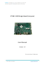
VT-SBC-3399
Brand: Vantron Pages: 44

BNX-E38
Brand: BESTEK Pages: 48

VIM1S
Brand: KHADAS Pages: 4

SB586TCP/166
Brand: ICS Pages: 128

CPB902
Brand: Fastwel Pages: 91

TMS320DM335
Brand: Texas Instruments Pages: 172

Armadillo-9 AN010
Brand: Atmark Techno Pages: 37

VAR-OM35CustomBoard v2.3
Brand: Variscite Pages: 8

A13-OLinuXino
Brand: OLIMEX Pages: 37

ClearFog
Brand: SolidRun Pages: 22

3.5-SBC-KBL
Brand: Kontron Pages: 7

SBC AXEL
Brand: Dave Embedded Systems Pages: 139


